


TUNER 737694 AT349357054
With prescaler U665B
ELKO UNIT - BS1451 ET309378047
ST-BY SUPPLY - BS613 ET309309977
PLL SYNTHESIZER TUNING CONTROL BS656 AT349354169
with U3870 -Bit Microcontroller-Microcomputer - Plus 70 instruction set & binary timer
Vishay Telefunken
8-Bit Microcontrollers,Timers
Clock Frequency - Max. (Hz)=4.0M
Clock Frequency - Min. (Hz)=2.0M
Min Instruction Length (bits)=8
Max Instruction Length (bits)=24
Memory Addressing Range=64k
Number of Addressing Modes=5
On-Chip RAM (Bytes)=0
On-Chip ROM (bytes)=1.0k
Number of Interrupt Lines=1
No. of Non-Maskable Interrupts=0
Number of Maskable Interrupts=1
Number of I/O Lines=32
No. of I/O Ports=4
Vsup Nom.(V) Supply Voltage=5.0
Package=DIP
Pins=40
Military=N
Technology=NMOS
+ U3060 + ER1450 EAROM
VIDEO AT349354181
With TDA3562A

The TDA3562A is a monolithic IC designed as
decode PAL and/or NTSC colour television standards
and it combines all functions required for the
identification and demodulation of PAL and NTSC
signals.
.CHROMINANCE SIGNALPROCESSOR
.LUMINANCE SIGNAL PROCESSING WITH
CLAMPING
.HORIZONTAL AND VERTICAL BLANKING
.LINEAR TRANSMISSION OF INSERTED
RGB SIGNALS
.LINEAR CONTRAST AND BRIGHTNESS
CONTROL ACTING ON INSERTED AND MATRIXED
SIGNALS
.AUTOMATIC CUT-OFF CONTROL
.NTSC HUE CONTROL.
TELEFUNKEN PALCOLOR V3210 CHASSIS 415 A 1
TELEFUNKEN PLL SYNTHESIZER Digital phase control circuit including an auxiliary circuit
An electronically controllable tuning device includes a voltage controlled oscillator adapted to have an oscillation frequency controlled by a control voltage and simultaneously generate a fundamental wave of a predetermined frequency, a programmable frequency divider for dividing the fundamental wave frequency at a frequency division ratio corresponding to the control of a channel selection means and a phase locked loop adapted to compare the fundamental wave phase with the phase of the output of the programmable divider to generate a comparison output and feeding the comparison output back to the voltage controlled oscillator to control the output frequency of the voltage controlled oscillator. The tuning device further includes means for supplying as a local oscillation signal to an intermediate frequency generating mixer one of higher harmonic wave components of the fundamental wave.
 A digital phase control circuit which includes a controllable oscillator, a programmable divider coupled to the oscillator, a reference frequency source, a phase discriminator coupled to the outputs of the programmable divider and reference frequency source and means coupling the output of the phase discriminator to a control input of the oscillator. In addition to these components, an auxiliary circuit is provided which has its input coupled to the output of the phase discriminator and first and second outputs coupled to the reference frequency source and the programmable divider. The auxiliary circuit generates a first signal at the input of the reference frequency source when the phase difference between the signals at the outputs of the programmable divider and the reference frequency source is in one direction and a second signal at the second input of the programmable divider when the phase difference is in the opposite direction.
 1. In a digital phase control circuit including a controllable oscillator having a control input; a programmable first divider having first and second inputs, said first input being coupled to the output of said oscillator; a reference frequency source comprising a second divider having an input; a phase discriminator having first and second inputs coupled to the outputs of said programmable first divider and said second divider respectively, said phase discriminator further having output means; and means coupling the output means of said phase discriminator to the control input of said controllable oscillator, the frequency of said oscillator being controlled in a direction determined by the direction of the phase deviation between the signals applied to the first and second inputs of said phase discriminator and compared therein; the improvement comprising:
an auxiliary circuit having input means coupled to the output means of said phase discriminator, a first output coupled to the input of said second divider comprising said reference frequency source and a second output coupled to the second input of said programmable first divider, said auxiliary circuit generating a first synchronizing signal at the input of said second divider when the phase difference between the signals at the ou
tputs of said programmable first divider and said second divider is in one direction and generating a second synchronizing signal at the second input of said programmable first divider when the phase difference between the signals at the outputs of said programmable first divider and said second divider is in the opposite direction thereby setting either said programmable first divider or said second divider, respectively, to a predetermined initial phase position, the divider set to said predetermined initial phase position being maintained in said position until the other divider reaches its predetermined initial phase position.2. The phase control circuit defined by claim 1 wherein said auxiliary circuit comprises a clock pulse generator for generating a signal at a predetermined interval after generation of a signal at the output of said phase discriminator, an auxiliary circuit output signal being generated at the input of said second divider or at the input of said programmable first divider only if the signal at the output of said phase discriminator is generated for an interval longer than said predetermined interval. 3. The phase control circuit defined by claim 2 wherein the output of said phase discriminator and the output of said auxiliary circuit each comprise a plurality of sequential pulses having a leading edge and a trailing edge, the leading edges of the pulses at the output of said auxiliary circuit occurring later than the leading edges of the corresponding pulses at the output of said phase discriminator, and the trailing edges of the corresponding pulses at both the output of the auxiliary circuit and the output of the phase discriminator coinciding. 4. The phase control circuit defined by claim 2 wherein said clock pulse generator receives counting pulses at a constant frequency, means are provided for releasing said clock pulse generator to count said counting pulses from its predetermined initial position when a signal is generated at the output of said phase discriminator and means are provided for coupling the signal at the output of said clock pulse generator to a disable input thereof to stop said counter. 5. A phase control circuit as defined by claim 4 wherein the output means of said phase discriminator comprises a first output at which pulses appear when the frequency of said oscillator is increasing and a second output at which pulses appear when the frequency of said oscillator is decreasing, and wherein said auxiliary circuit further includes a first gating circuit having first and second inputs coupled to the first and second outputs of said phase discriminator and an output coupled to a reset terminal of said clock pulse generator, second and third gating circuits for coupling the output of said clock pulse generator to the input of said second divider and to the second input of said programmable first divider, respectively, and fourth and fifth gating circuits coupling the first and second outputs of said
phase discriminator to the inputs of said second and third gating circuits.
Description:
BACKGROUND OF THE INVENTION
This invention relates to digital phase control circuits and, in particular, to a phase control circuit which has improved transient response during its readjustment mode.
Digital phase control circuits are known which include a controllable oscillator, a programmable divider, a reference frequency source, a phase discriminator and a lowpass filter or integrating circuit. The output signal of the controllable oscillator is fed to one input of the phase discriminator via the programmable divider and the other input of the phase discriminator receives a signal from the reference frequency source. The low-pass filter circuit derives a control signal from the output of the phase discriminator so as to control the controllable oscillator.
The signals at the output of the phase discriminator have rectangular pulses. The average d.c. voltage of the rectangular pulses is obtained by means of the series-connected filter circuit which provides a setting voltage for the controllable oscillator. The circuit regulates itself in such a way that, in the steady-state, the signals applied to the phase discriminator coincide in frequency and phase.
In order to prevent excessive overshoot of the controllable oscillator, a minimum time constant is required in the filter circuit which may be designed, for example, as an active integrator. This results in a relatively long time constant for the entire system which can be detrimental in many cases. A long time constant may also increase the tendency toward resonance of the entire circuit.
It is an object of the present invention to provide a phase control circuit which is substantially improved with respect to its transient response during readjustment.
SUMMARY OF THE INVENTION
The present invention comprises a digital phase control circuit which includes a controllable oscillator, a programmable divider coupled to the oscillator, a reference frequency source, a phase discriminator coupled to the outputs of the programmable divider and reference frequency source and means coupling the output of the phase discriminator to a control input of the oscillator. In addition to these components, an auxiliary circuit is provided which has its input coupled to the output of the phase discriminator and first and second outputs coupled to the reference frequency source and the programmable divider. The auxiliary circuit generates a first signal at the input of the reference frequency source when the phase difference between the signals at the outputs of the programmable divider and the reference frequency source are in one direction and a second signal at the second input of the programmable divider when the phase difference is in the opposite direction.
Thus, in the present invention, an auxiliary circuit is provided in addition to the components of the prior art phase control circuit. This auxiliary circuit acts selectively on the programmable divider or the reference frequency source to reset the programmable divider or the reference frequency source, respectively, to a predetermined initial phase position at specific points in time. This initiates a comparison which begins at the predetermined initial phase position of the circuit. The comparison process beginning with the return of the predetermined initial position of the programmable divider or of the reference frequency source is repeated continuously. The invention operates such that, during every comparison cycle, a genuine phase or frequency comparison is effected between the two signals present at the phase discriminator. Each time at the start of the comparison cycle, the phase difference is defined as "zero." Therefore, the phase of frequency deviation present at the end of the comparison cycle between the two signals present at the phase discriminator is an exact measure of the phase deviation.
BRIEF DESCRIPTION OF THE DRAWINGS
FIG. 1 shows a phase control circuit in accordance with the present invention.
FIGS. 2 and 3 show the output signals of a prior art phase control circuit for both directions of adjustment.
FIG. 4 is a pulse diagram of the signals in a phase control circuit including the features of the present invention for one direction of adjustment.
FIG. 5 shows signals corresponding to FIG. 4 for the other direction of adjustment.
FIG. 6 is a waveform diagram comparing the operation of the circuit with and without the auxiliary circuit of FIG. 1.
FIG. 7 shows an embodiment of the auxiliary circuit of FIG. 1.
FIG. 8 shows a television tuner constructed in accordance with the invention.
DESCRIPTION OF THE PREFERRED EMBODIMENTS
FIG. 1 is a block diagram showing a phase adjustment circuit which includes a voltage controllable oscillator 1 (VCO), a programmable divider 2, a reference source 4, a phase discriminator 3, a coupling circuit 6 and a l owpass filter and amplifier circuit 5. These components are combined in a known manner to form a control loop. The programmable divider can be set to a selected dividing ratio which determines the initial frequency of the controllable oscillator 1. The programmable divider may also have fixed predividers (not shown) connected between it and the oscillator 1. The reference frequency source 4 includes a quartz oscillator 4a and a series-connected frequency divider 4b having, for example, a fixed dividing ratio. The output signal of the divider 4b is fed to the phase discriminator 3 to provide a reference signal.
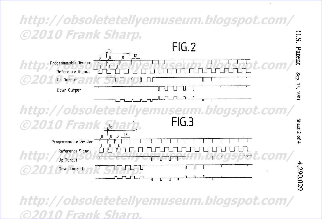
Before describing auxiliary circuit 7 of FIG. 1, the operation of the prior art phase control circuit will be explained with the aid of FIGS. 2 and 3; that is, the circuit shown in FIG. 1 without the auxiliary circuit 7 will be described.
The output signal of the programmable divider 2 is shown at the top of FIG. 2. After each passage through the programmable divider 2, a negative pulse 8 appears at the output of this divider and is fed to the phase discriminator 3. In the second line of FIG. 2, the reference signal is shown which is fed to the other input of the phase discriminator 3.
The phase discriminator 3 has an output 9 at which control pulses appear when the oscillator 1 is adjusted in the upward direction; that is, toward a higher frequency, and an output 10 at which pulses appear for an adjustment in the downward or lower frequency direction. The signals at outputs 9 and 10 are illustrated in the third and fourth lines of FIG. 2. The last line shows a so-called "tristate signal" which is obtained at the output of coupling circuit 6 and which is fed to the lowpass filter 5. The diagram shown in FIG. 2 is based on a so-called Type 4 phase discriminator which is described at page 19 of the book by Horst Geschwinde "Einfuhrung in die PLL-Technik" (Introduction to the PLL Technique), published by Vieweg. Each of the outputs 9 and 10 of the phase discriminator 3 has an associated output in a bistable circuit comprising the phase discriminator. In the illustrated case, the phase discrimin
 ator 3 is designed so that the bistable circuits respond to the negative-going edge of the pulse 8 coming from the programmed divider 2. If there is a phase difference between the signals applied to the phase discriminator 3, pulses appear either at the "upward" output 9 or at the "downward" output 10, depending on the direction of the deviation. The bistable circuit associated with the "upward" output can be set by the edges 11 of the reference signal and reset by the pulses 8 coming from tne programmable divider 2. Conversely, the bistable circuit in the phase discriminator associated with the "downward" output can be set exactly oppositely by the pulses 8 coming from the programmable divider 2 and reset by the edges 11 of the reference signal.
FIG. 2 shows the signals for the case where at time t 0 the dividing ratio of the programmable divider 2 is switched to a higher value. Consequently, the frequency of the oscillator 1 is adjusted toward higher frequencies, which can be seen in FIG. 2 in that the pulses 8 at the output of the programmable divider jump toward a lower frequency after a new dividing ratio has been set into the programmable divider and thereafter are brought closer together by the adjustment process. Thus, at an interval indicated by the bracket 12, the frequency of the pulses coincides with the frequency of the reference signals but there still exists a phase deviation between the signals. This deviation can be overcome by temporarily increasing the frequency of the signal of oscillator 1 beyond the desired value. For that reason, the pulses at the "upward" output 9 continue to be generated. The prior art circuit thus exhibits an overshoot which is required by the system.
FIG. 3 is a pulse diagram in which the dividing ratio of the programmable divider 2 of FIG. 1 is set to a lower value at time t 0 . The time at w hich coincidence with respect to frequency exists for the signals being compared in the phase discriminator is identified by a bracket 13. The operation of the prior art system under these conditions is analagous to the previously described operation under the conditions of FIG. 2.
The auxiliary circuit 7 of FIG. 1 resets the programmable divider 2 or the reference frequency source 4, to its initial position at specific points in time. The auxiliary circuit 7 is controlled by the signals at outputs 9 and 10 of the phase discriminator 3.
FIGS. 4 and 5 show how the auxiliary circuit of FIG. 1 controls the programmable divider 2 and the reference frequency source 4. FIG. 4 illustrates the operation of the circuit including auxiliary circuit 7 for a change in frequency corresponding to FIG. 2 wherein the oscillator frequency increases; that is, changes in the upward direction. It is assumed that the circuit has the same components as the circuits on which FIGS. 2 and 3 are based but that it includes in addition the auxiliary circuit 7.
The synchronizing signal A shown in the last line of FIG. 4 is generated by the auxiliary circuit 7. The synchronizing signal A includes pulses 14 and 17 which are fed to the reset input R of the reference frequency source. At time t 0 , a new dividing ratio is fed into the programmable divider 2 and at time t 1 the oscillator begins to increase its frequency so that the pulses 8 come closer together again. At time t 1 , the pulse 15 is initiated at the "upward" output 9 of the phase discriminator since the edge 11 of the reference signal appears earlier than the next pulse 8 from the programmable divider. The pulse 14 of the synchronizing signal A is derived from the pulse 15.
Pulse 14 is used initially to reset the divider 4b of the reference frequency source 4 which does not generate reference signal pulses as long as pulse 14 is present. At time t 2 , the pulse 15 and the output pulse 14 derived from pulse 15 are terminated. Thus, at time t 2 , the divider of the frequency source 4 is restarted from its basic position.
The frequency divider 4b may be a twelve bit divider consisting, for example, of two type CD4520 integrated circuits manufactured by RCA. This known divider is set to its basic position by a logical reset signal.
After a period T 1 of the reference signal, at time t 3 , a new control pulse 16 starts at the output 9 of the phase discriminator 3 since the edge 11 again appears earlier than the next pulse 8 from the programmable divider. A synchronizing pulse 17 is again generated which sets back the divider 4b of the reference frequency source 4 and stops it.
The adjustment is effected in the above-described manner until at time t 4 the signals being compared in the phase discriminator 3 coincide with respect to frequency and phase. As can be seen from a comparison of FIG. 4 with FIG. 2, this state is attained much faster than in the circuit without the auxiliary circuit 7. The control pulse terminated each time at the end of the comparison cycle provides a precise indication of the frequency deviation of the two signals applied to the phase discriminator, which is not the case in FIGS. 2 and 3.
Upon a change in the frequency of the oscillator in the opposite direction (downward), a synchronizing signal B is generated in the auxiliary circuit 7, as shown in FIG. 5, from the signal at "downward" output 10 of phase discriminator 3. With this synchronizing signal, the programmable divider 2 is controlled rather than the reference source 4 as shown in FIG. 4.
At time t 0 , as in FIG. 3, the dividing ratio of the programmable divider is reduced to correspond to the reduction in frequency of the oscillator 1. This initially effects an increase in the output frequency of the controllable oscillator. The synchronizing signal B is derived from the pulses 18 and 19 at the "downward" output 10 of the discriminator 3. This signal is fed to the load input L of the programmable divider 2. At time t 1 a pulse 8 from the programmable divider starts the pulse 18 at the output 10. The programmable divider is set by the synchronizing pulse 20 derived from pulse 18 and is kept in the initial position until time t 2 . At time t 2 , the edge 11 of the reference signal terminates the pulse 18. At the same time, the programmable divider begins to operate again. At t 3 , the pulse 19 at the output 10 is started because the next pulse 8 appears earlier than the next negative-going edge 11 of the reference signal. The synchronizing pulse 21 derived from pulse 19 again sets the programmable divider 2 and holds it in its initial position. At time t 4 the programmable divider 2 is released again and the process continues.
The programmable divider 2 is a known component. For example, four type 74 LS169 integrated circuits manufactured by National Semiconductor may be used in series as a fourteen bit presettable down counter.
As is evident from the explanation of FIGS. 4 and 5, the reference frequency source 4 is controlled by the auxiliary circuit in one direction and the programmable divider 2, located between the oscillator 1 and the discriminator 3, in the other direction. The influenced circuit is controlled in accordance with the signals appearing at the output of the discriminator 3, which correspond to the phase or frequency error, so that at the beginning of each comparison cycle the phase error is assumed to be zero. In this way, adjustment of the circuit beyond the desired value is avoided. Thus, the described phase control circuit, including the auxiliary circuit 7, has very short transient periods.
FIGS. 4 and 5 show that the rising edge of the synchronizing signals A and B are shifted by the time τ with respect to the associated output signal of discriminator 3. By providing a predetermined delay period τ, the auxiliary circuit 7 is made effective for only a certain minimum width of the pulses of the output signal from discriminator 3. If the pulses at outputs 9 and 10 of the discriminator 3 fall below this minimum width, no synchronizing signals A or B are generated any longer. The circuit then operates in the customary manner, as described in connection with FIGS. 2 and 3. The delay period is advantageously selected to be greater than one period of the frequency of the reference oscillator so that the auxiliary circuit will not respond to the non-transient state.
If such a delay period is provided, the control circuit will be brought into a state, by means of the auxiliary circuit 7 provided to avoid overshooting, in which the signals present at the phase discriminator coincide with respect to frequency as well as phase. Then the auxiliary circuit 7 is no longer effective.
FIG. 6 shows the result obtained with the auxiliary circuit 7 by illustrating the control signal for oscillator 1. The top portion of FIG. 6 shows the signal obtained when an auxiliary circuit was used which operates in the manner described above under conditions of increasing frequency. The signal at the bott om of FIG. 6 was obtained when the same circuit was used without auxiliary circuit 7. It can be seen that the auxiliary circuit 7 resulted in a significant improvement in the transient behavior.
FIG. 7 shows an embodiment of the auxiliary circuit 7 of FIG. 1. The auxiliary circuit includes a counter 22 and logic gates 23 to 27, the counter generating the fixed delay period λ. A typical counter which may be used for this purpose is the type CD4520 manufactured by RCA. The signals at the outputs 9 and 10 of the phase discriminator 3 are fed through an AND gate 23 to the reset input of the counter 22. The clock pulse input of the counter 22 receives, via an input terminal 30, counting pulses at a frequency of, for example, 1 MHz. If no pulse arrives from the outputs 9 and 10 of the phase discriminator, the reset input receives a reset signal and the clock pulses at the clock pulse input of the counter 22 are ineffective. The output Q n of the n th stage of the counter 22 is connected with a disable input D of the counter. That is, if the counter state Q n is reached, the counter stops itself. The synchronizing signals A and B are also derived from output Q n via gates 25 and 27. A signal is fed via inverters 24 and 26, to the gates 25 and 27 which act as gating circuits so as to indicate which one of the two gates 25 and 27 is to be enabled for the signal coming from output Q n . Gates 25 and 27 therefore control whether the programmable divider 2 or the reference frequency source 4 of FIG. 1 receives a synchronizing signal.
With reference to FIGS. 4 and 5, the circuit in FIG. 7 operates as follows: The pulse 15 in FIG. 4 is present at the input 9 and enables gate 27 via inverter 26 to provide a synchronizing signal. However, no pulse appears at output 29 because the output Q n of the counter 22 does not furnish a signal. Pulse 15 cancels the reset signal of counter 22 and counting pulses from input 30 are counted into the counter. After a delay period λ a signal jump appears at the output Q n , in accordance with the clock pulse frequency and the number of stages in the counter, which stops the counter 22 through the disable input. The change of signals at the output Q n also changes the logic state at the upper input of gate 27 so that the pulse 14 of FIG. 4 is formed. As soon as pulse 15 in FIG. 4 is completed, the AND condition for gate 27 is no longer met so that the pulse 14 is terminated simultaneously with pulse 15. The termination of pulse 15 causes the counter 22 to be reset to its starting position and held in that position.
When there is a pulse at input 10 of the circuit of FIG. 7, the circuit operates in a corresponding manner with the difference that gate 25 is enabled instead of gate 27. In this case, the synchronizing signal B is formed at output 28 and used to control the programmable divider 2. By selecting the frequency of the counting clock pulse at the input 30 it is possible to preselect the delay period λ.
It is also possible to obtain the delay period λ by means of circuit elements which operate in a different manner. For example, the delay of a plurality of series-connected gates (e.g., inverters) can be utilized.
FIG. 8 shows the complete circuit diagram of a tuner embodying the features of the present invention. At the top left of FIG. 1, block 31 is a tuner including the VCO 1. The signal from the VCO 1 travels through a predivider 32 included in the tuner to the programmable divider 2. At the beginning of a dividing cycle, the programmable divider is set to the preprogrammed value via a "load" input L and is then pulsed until it reaches the value zero. When it reaches the value zero, the load input receives a new charging pulse via a gate 33 with which the starting position of the programmable divider 2 is reset. The charging pulse of the programmable divider is fed to the input 35 of a phase discriminator 3 which is shown in dashed lines in FIG. 8. The other input 34 of the phase discriminator 3 receives a signal from the reference divider 4. The phase discriminator 3 which operates in a known manner, includes a plurality of gates.
At the lower right of FIG. 8, the coupling circuit 6 is shown. The auxiliary circuit 7 which has already been described in connection with FIG. 7 is shown in outline in FIG. 8. The synchronizing signal A is fed to the reset input of the reference divider 4 and the synchronizing signal B is fed to gate 33.
The auxiliary circuit 7 is also connected to a lock indicator which includes a counter 36, an AND gate 37 and an inverter 38. The counter 36 is set back with each synchronizing signal A and B via a reset input. Clock pulses at a relatively low frequency are fed to the clock pulse input of the counter 36 via an AND gate 37. These clock pulses are obtained from the output of the reference divider 4. From an output Q p , a lock signal is derived. This lock signal appears only if no synchronizing signal appears for a relatively long period of time. The supply of clock pulses through gate 37 is blocked as soon as the lock signal appears because of the feedback of the lock signal via an inverter 38. The lock signal remains in effect until a new synchronizing signal is formed.
The lower left of FIG. 8 shows the filter circuit 5 which includes an operational amplifier 39.
It will be understood that the above description of the present invention is susceptible to various modifications, changes and adaptations, and the same are intended to be comprehended within the meaning and range of equivalents of the appended claims.
This invention relates to digital phase control circuits and, in particular, to a phase control circuit which has improved transient response during its readjustment mode.
Digital phase control circuits are known which include a controllable oscillator, a programmable divider, a reference frequency source, a phase discriminator and a lowpass filter or integrating circuit. The output signal of the controllable oscillator is fed to one input of the phase discriminator via the programmable divider and the other input of the phase discriminator receives a signal from the reference frequency source. The low-pass filter circuit derives a control signal from the output of the phase discriminator so as to control the controllable oscillator.
The signals at the output of the phase discriminator have rectangular pulses. The average d.c. voltage of the rectangular pulses is obtained by means of the series-connected filter circuit which provides a setting voltage for the controllable oscillator. The circuit regulates itself in such a way that, in the steady-state, the signals applied to the phase discriminator coincide in frequency and phase.
In order to prevent excessive overshoot of the controllable oscillator, a minimum time constant is required in the filter circuit which may be designed, for example, as an active integrator. This results in a relatively long time constant for the entire system which can be detrimental in many cases. A long time constant may also increase the tendency toward resonance of the entire circuit.
It is an object of the present invention to provide a phase control circuit which is substantially improved with respect to its transient response during readjustment.
SUMMARY OF THE INVENTION
The present invention comprises a digital phase control circuit which includes a controllable oscillator, a programmable divider coupled to the oscillator, a reference frequency source, a phase discriminator coupled to the outputs of the programmable divider and reference frequency source and means coupling the output of the phase discriminator to a control input of the oscillator. In addition to these components, an auxiliary circuit is provided which has its input coupled to the output of the phase discriminator and first and second outputs coupled to the reference frequency source and the programmable divider. The auxiliary circuit generates a first signal at the input of the reference frequency source when the phase difference between the signals at the outputs of the programmable divider and the reference frequency source are in one direction and a second signal at the second input of the programmable divider when the phase difference is in the opposite direction.
Thus, in the present invention, an auxiliary circuit is provided in addition to the components of the prior art phase control circuit. This auxiliary circuit acts selectively on the programmable divider or the reference frequency source to reset the programmable divider or the reference frequency source, respectively, to a predetermined initial phase position at specific points in time. This initiates a comparison which begins at the predetermined initial phase position of the circuit. The comparison process beginning with the return of the predetermined initial position of the programmable divider or of the reference frequency source is repeated continuously. The invention operates such that, during every comparison cycle, a genuine phase or frequency comparison is effected between the two signals present at the phase discriminator. Each time at the start of the comparison cycle, the phase difference is defined as "zero." Therefore, the phase of frequency deviation present at the end of the comparison cycle between the two signals present at the phase discriminator is an exact measure of the phase deviation.
BRIEF DESCRIPTION OF THE DRAWINGS
FIG. 1 shows a phase control circuit in accordance with the present invention.
FIGS. 2 and 3 show the output signals of a prior art phase control circuit for both directions of adjustment.
FIG. 4 is a pulse diagram of the signals in a phase control circuit including the features of the present invention for one direction of adjustment.
FIG. 5 shows signals corresponding to FIG. 4 for the other direction of adjustment.
FIG. 6 is a waveform diagram comparing the operation of the circuit with and without the auxiliary circuit of FIG. 1.
FIG. 7 shows an embodiment of the auxiliary circuit of FIG. 1.
FIG. 8 shows a television tuner constructed in accordance with the invention.
DESCRIPTION OF THE PREFERRED EMBODIMENTS
FIG. 1 is a block diagram showing a phase adjustment circuit which includes a voltage controllable oscillator 1 (VCO), a programmable divider 2, a reference source 4, a phase discriminator 3, a coupling circuit 6 and a l
owpass filter and amplifier circuit 5. These components are combined in a known manner to form a control loop. The programmable divider can be set to a selected dividing ratio which determines the initial frequency of the controllable oscillator 1. The programmable divider may also have fixed predividers (not shown) connected between it and the oscillator 1. The reference frequency source 4 includes a quartz oscillator 4a and a series-connected frequency divider 4b having, for example, a fixed dividing ratio. The output signal of the divider 4b is fed to the phase discriminator 3 to provide a reference signal. Before describing auxiliary circuit 7 of FIG. 1, the operation of the prior art phase control circuit will be explained with the aid of FIGS. 2 and 3; that is, the circuit shown in FIG. 1 without the auxiliary circuit 7 will be described.
The output signal of the programmable divider 2 is shown at the top of FIG. 2. After each passage through the programmable divider 2, a negative pulse 8 appears at the output of this divider and is fed to the phase discriminator 3. In the second line of FIG. 2, the reference signal is shown which is fed to the other input of the phase discriminator 3.
The
 phase discriminator 3 has an output 9 at which control pulses appear when the oscillator 1 is adjusted in the upward direction; that is, toward a higher frequency, and an output 10 at which pulses appear for an adjustment in the downward or lower frequency direction. The signals at outputs 9 and 10 are illustrated in the third and fourth lines of FIG. 2. The last line shows a so-called "tristate signal" which is obtained at the output of coupling circuit 6 and which is fed to the lowpass filter 5. The diagram shown in FIG. 2 is based on a so-called Type 4 phase discriminator which is described at page 19 of the book by Horst Geschwinde "Einfuhrung in die PLL-Technik" (Introduction to the PLL Technique), published by Vieweg. Each of the outputs 9 and 10 of the phase discriminator 3 has an associated output in a bistable circuit comprising the phase discriminator. In the illustrated case, the phase discriminator 3 is designed so that the bistable circuits respond to the negative-going edge of the pulse 8 coming from the programmed divider 2. If there is a phase difference between the signals applied to the phase discriminator 3, pulses appear either at the "upward" output 9 or at the "downward" output 10, depending on the direction of the deviation. The bistable circuit associated with the "upward" output can be set by the edges 11 of the reference signal and reset by the pulses 8 coming from tne programmable divider 2. Conversely, the bistable circuit in the phase discriminator associated with the "downward" output can be set exactly oppositely by the pulses 8 coming from the programmable divider 2 and reset by the edges 11 of the reference signal.
 FIG. 2 shows the signals for the case where at time t 0 the dividing ratio of the programmable divider 2 is switched to a higher value. Consequently, the frequency of the oscillator 1 is adjusted toward higher frequencies, which can be seen in FIG. 2 in that the pulses 8 at the output of the programmable divider jump toward a lower frequency after a new dividing ratio has been set into the programmable divider and thereafter are brought closer together by the adjustment process. Thus, at an interval indicated by the bracket 12, the frequency of the pulses coincides with the frequency of the reference signals but there still exists a phase deviation between the signals. This deviation can be overcome by temporarily increasing the frequency of the signal of oscillator 1 beyond the desired value. For that reason, the pulses at the "upward" output 9 continue to be generated. The prior art circuit thus exhibits an overshoot which is required by the system.
FIG. 3 is a pulse diagram in which the dividing ratio of the programmable divider 2 of FIG. 1 is set to a lower value at time t 0 . The time at w
 hich coincidence with respect to frequency exists for the signals being compared in the phase discriminator is identified by a bracket 13. The operation of the prior art system under these conditions is analagous to the previously described operation under the conditions of FIG. 2.
 The auxiliary circuit 7 of FIG. 1 resets the programmable divider 2 or the reference frequency source 4, to its initial position at specific points in time. The auxiliary circuit 7 is controlled by the signals at outputs 9 and 10 of the phase discriminator 3.
FIGS. 4 and 5 show how the auxiliary circuit of FIG. 1 controls the programmable divider 2 and the reference frequency source 4. FIG. 4 illustrates the operation of the circuit including auxiliary circuit 7 for a change in frequency corresponding to FIG. 2 wherein the oscillator frequency increases; that is, changes in the upward direction. It is assumed that the circuit has the same components as the circuits on which FIGS. 2 and 3 are based but that it includes in addition the auxiliary circuit 7.
The synchronizing signal A shown in the last line of FIG. 4 is generated by the auxiliary circuit 7. The synchronizing signal A includes pulses 14 and 17 which are fed to the reset input R of the reference frequency source. At time t 0 , a new dividing ratio is fed into the programmable divider 2 and at time t 1 the oscillator begins to increase its frequency so that the pulses 8 come closer together again. At time t 1 , the pulse 15 is initiated at the "upward" output 9 of the phase discriminator since the edge 11 of the reference signal appears earlier than the next pulse 8 from the programmable divider. The pulse 14 of the synchronizing signal A is derived from the pulse 15.
Pulse 14 is used initially to reset the divider 4b of the reference frequency source 4 which does not generate reference signal pulses as long as pulse 14 is present. At time t 2 , the pulse 15 and the output pulse 14 derived from pulse 15 are terminated. Thus, at time t 2 , the divider of the frequency source 4 is restarted from its basic position.
The frequency divider 4b may be a twelve bit divider consisting, for example, of two type CD4520 integrated circuits manufactured by RCA. This known divider is set to its basic position by a logical reset signal.
After a period T 1 of the reference signal, at time t 3 , a new control pulse 16 starts at the output 9 of the phase discriminator 3 since the edge 11 again appears earlier than the next pulse 8 from the programmable divider. A synchronizing pulse 17 is again generated which sets back the divider 4b of the reference frequency source 4 and stops it.
The adjustment is effected in the above-described manner until at time t 4 the signals being compared in the phase discriminator 3 coincide with respect to frequency and phase. As can be seen from a comparison of FIG. 4 with FIG. 2, this state is attained much faster than in the circuit without the auxiliary circuit 7. The control pulse terminated each time at the end of the comparison cycle provides a precise indication of the frequency deviation of the two signals applied to the phase discriminator, which is not the case in FIGS. 2 and 3.
Upon a change in the frequency of the oscillator in the opposite direction (downward), a synchronizing signal B is generated in the auxiliary circuit 7, as shown in FIG. 5, from the signal at "downward" output 10 of phase discriminator 3. With this synchronizing signal, the programmable divider 2 is controlled rather than the reference source 4 as shown in FIG. 4.
At time t 0 , as in FIG. 3, the dividing ratio of the programmable divider is reduced to correspond to the reduction in frequency of the oscillator 1. This initially effects an increase in the output frequency of the controllable oscillator. The synchronizing signal B is derived from the pulses 18 and 19 at the "downward" output 10 of the discriminator 3. This signal is fed to the load input L of the programmable divider 2. At time t 1 a pulse 8 from the programmable divider starts the pulse 18 at the output 10. The programmable divider is set by the synchronizing pulse 20 derived from pulse 18 and is kept in the initial position until time t 2 . At time t 2 , the edge 11 of the reference signal terminates the pulse 18. At the same time, the programmable divider begins to operate again. At t 3 , the pulse 19 at the output 10 is started because the next pulse 8 appears earlier than the next negative-going edge 11 of the reference signal. The synchronizing pulse 21 derived from pulse 19 again sets the programmable divider 2 and holds it in its initial position. At time t 4 the programmable divider 2 is released again and
the process continues. The programmable divider 2 is a known component. For example, four type 74 LS169 integrated circuits manufactured by National Semiconductor may be used in series as a fourteen bit presettable down counter.
As is evident from the explanation of FIGS. 4 and 5, the reference frequency source 4 is controlled by the auxiliary circuit in one direction and the programmable divider 2, located between the oscillator 1 and the discriminator 3, in the other direction. The influenced circuit is controlled in accordance with the signals appearing at the output of the discriminator 3, which correspond to the phase or frequency error, so that at the beginning of each comparison cycle the phase error is assumed to be zero. In this way, adjustment of the circuit beyond the desired value is avoided. Thus, the described phase control circuit, including the auxiliary circuit 7, has very short transient periods.
FIGS. 4 and 5 show that the rising edge of the synchronizing signals A and B are shifted by the time τ with respect to the associated output signal of discriminator 3. By providing a predetermined delay period τ, the auxiliary circuit 7 is made effective for only a certain minimum width of the pulses of the output signal from discriminator 3. If the pulses at outputs 9 and 10 of the discriminator 3 fall below this minimum width, no synchronizing signals A or B are generated any longer. The circuit then operates in the customary manner, as described in connection with FIGS. 2 and 3. The delay period is advantageously selected to be greater than one period of the frequency of the reference oscillator so that the auxiliary circuit will not respond to the non-transient state.
If such a delay period is provided, the control circuit will be brought into a state, by means of the auxiliary circuit 7 provided to avoid overshooting, in which the signals present at the phase discriminator coincide with respect to frequency as well as phase. Then the auxiliary circuit 7 is no longer effective.
FIG. 6 shows the result obtained with the auxiliary circuit 7 by illustrating the control signal for oscillator 1. The top portion of FIG. 6 shows the signal obtained when an auxiliary circuit was used which operates in the manner described above under conditions of increasing frequency. The signal at the bott
 om of FIG. 6 was obtained when the same circuit was used without auxiliary circuit 7. It can be seen that the auxiliary circuit 7 resulted in a significant improvement in the transient behavior.
 FIG. 7 shows an embodiment of the auxiliary circuit 7 of FIG. 1. The auxiliary circuit includes a counter 22 and logic gates 23 to 27, the counter generating the fixed delay period λ. A typical counter which may be used for this purpose is the type CD4520 manufactured by RCA. The signals at the outputs 9 and 10 of the phase discriminator 3 are fed through an AND gate 23 to the reset input of the counter 22. The clock pulse input of the counter 22 receives, via an input terminal 30, counting pulses at a frequency of, for example, 1 MHz. If no pulse arrives from the outputs 9 and 10 of the phase discriminator, the reset input receives a reset signal and the clock pulses at the clock pulse input of the counter 22 are ineffective. The output Q n of the n th stage of the counter 22 is connected with a disable input D of the counter. That is, if the counter state Q n is reached, the counter stops itself. The synchronizing signals A and B are also derived from output Q n via gates 25 and 27. A signal is fed via inverters 24 and 26, to the gates 25 and 27 which act as gating circuits so as to indicate which one of the two gates 25 and 27 is to be enabled for the signal coming from output Q n . Gates 25 and 27 therefore control whether the programmable divider 2 or the reference frequency source 4 of FIG. 1 receives a synchronizing signal.
With reference to FIGS. 4 and
5, the circuit in FIG. 7 operates as follows: The pulse 15 in FIG. 4 is present at the input 9 and enables gate 27 via inverter 26 to provide a synchronizing signal. However, no pulse appears at output 29 because the output Q n of the counter 22 does not furnish a signal. Pulse 15 cancels the reset signal of counter 22 and counting pulses from input 30 are counted into the counter. After a delay period λ a signal jump appears at the output Q n , in accordance with the clock pulse frequency and the number of stages in the counter, which stops the counter 22 through the disable input. The change of signals at the output Q n also changes the logic state at the upper input of gate 27 so that the pulse 14 of FIG. 4 is formed. As soon as pulse 15 in FIG. 4 is completed, the AND condition for gate 27 is no longer met so that the pulse 14 is terminated simultaneously with pulse 15. The termination of pulse 15 causes the counter 22 to be reset to its starting position and held in that position. When there is a pulse at input 10 of the circuit of FIG. 7, the circuit operates in a corresponding manner with the difference that gate 25 is enabled instead of gate 27. In this case, the synchronizing signal B is formed at output 28 and used to control the programmable divider 2. By selecting the frequency of the counting clock pulse at the input 30 it is possible to preselect the delay period λ.
It is also possible to obtain the delay period λ by means of circuit elements which operate in a different manner. For example, the delay of a plurality of series-connected gates (e.g., inverters) can be utilized.
FIG. 8 shows the complete circuit diagram of a tuner embodying the features of the present invention. At the top left of FIG. 1, block 31 is a tuner including the VCO 1. The signal from the VCO 1 travels through a predivider 32 included in the tuner to the programmable divider 2. At the beginning of a dividing cycle, the programmable divider is set to the preprogrammed value via a "load" input L and is then pulsed until it reaches the value zero. When it reaches the value zero, the load input receives a new charging pulse via a gate 33 with which the starting position of the programmable divider 2 is reset. The charging pulse of the programmable divider is fed to the input 35 of a phase discriminator 3 which is shown in dashed lines in FIG. 8. The other input 34 of the phase discriminator 3 receives a signal from the reference divider 4. The phase discriminator 3 which operates in a known manner, includes a plurality of gates.
At the lower right of FIG. 8, the coupling circuit 6 is shown. The auxiliary circuit 7 which has already been described in connection with FIG. 7 is shown in outline in FIG. 8. The synchronizing signal A is fed to the reset input of the reference divider 4 and the synchronizing signal B is fed to gate 33.
The auxiliary circuit 7 is also connected to a lock indicator which includes a counter 36, an AND gate 37 and an inverter 38. The counter 36 is set back with each synchronizing signal A and B via a reset input. Clock pulses at a relatively low frequency are fed to the clock pulse input of the counter 36 via an AND gate 37. These clock pulses are obtained from the output of the reference divider 4. From an output Q p , a lock signal is derived. This lock signal appears only if no synchronizing signal appears for a relatively long period of time. The supply of clock pulses through gate 37 is blocked as soon as the lock signal appears because of the feedback of the lock signal via an inverter 38. The lock signal remains in effect until a new synchronizing signal is formed. The lower left of FIG. 8 shows the filter circuit 5 which includes an operational amplifier 39.
It will be understood that the above description of the present invention is susceptible to various modifications, changes and adaptations, and the same are intended to be comprehended within the meaning and range of equivalents of the appended claims.
TELEFUNKEN PALCOLOR V3210 CHASSIS 415 A 1 PLL MICROCOMPUTER Frequency synthesizer tuning system for television receivers:TFK u3870M
" A method for tuning a television receiver having automatic frequency control to the carrier frequency of a selected broadcast channel with an associated channel number including generating a variable frequency signal by means of a local oscillator, generating a reference frequency signal by means of a reference oscillator, and generating a local oscillator correction signal for matching an intermediate frequency signal derived from said local oscillator signal and the carrier frequency signal with a predetermined nominal intermediate frequency signal, said method being characterized by the use of a microcomputer and comprising:
generating binary signals representing first and second digital tune words, said digital tune words representing a selected channel;
storing said first and second digital tune words in a first data memory in said microcomputer;
reading said first and second digital tune words from said first memory and generating a divided-down local oscillator frequency by the use of said first digital tune word and a divided-down reference oscillator frequency by the use of said second digital tune word;
comparing said divided-down local oscillator and reference frequencies and generating a control signal representative of the difference in frequency of said divided-down local oscillator and reference frequencies;
coupling said control signal to said local oscillator for causing it to be locked to the frequency of said received carrier signal;
mixing the local oscillator frequency signal and the carrier frequency signal to generate an intermediate frequency signal;
comparing said intermediate frequency signal with said predetermined nominal intermediate frequency signal and providing a tuning voltage to said microcomputer, said tuning voltage being indicative of the magnitude and direction of a tuning error between said intermediate frequency signal and said predetermined nominal intermediate frequency signal;
incrementally adjusting the reference oscillator frequency by means of a tuning signal provided to said reference oscillator by said microcomputer in response to said tuning voltage;
detecting when the incrementally changing, divided-down reference oscillator frequency causes the intermediate frequency signal to pass said predetermined nominal intermediate frequency signal; and
incrementally stepping the divided-down reference oscillator frequency back a predetermined number of steps following the passage of said predetermined nominal intermediate frequency signal by said intermediate frequency signal in tuning said television receiver to the selected channel.
"

1. A tuning system for the tuner of a television receiver capable of receiving a composite television signal and including frequency discriminator (AFT) circuit means, said system including in combination:
a reference oscillator providing a reference signal at a predetermined frequency;
a local oscillator in the tuner providing a variable output frequency in response to the application of a control signal thereto;
a programmable frequency divider means having first and second inputs coupled respectively to the output of said reference oscillator and said local oscillator for producing signals on first and second outputs having frequencies which are a programmable fraction of the frequency of the signals applied to the inputs thereto;
phase comparator means having one input coupled with the first output of said programmable frequency divider means and having another input coupled with the second output of said programmable frequency divider means for developing a control signal and applying such control signal to said local oscillator for controlling the output frequency thereof;
counter circuit means coupled with said programmable frequency divider means for initially setting said divider means to a predetermined division ratio and operating to change the programmable fraction of division thereof in accordance with changes in the count in said counter circuit means;
control circuit means coupled with the output of said frequency discriminator means and further coupled with said counter circuit means for causing said counter circuit means to count at a first rate in a predetermined direction determined by the state of the output signal from said discriminator means in the absence of a predetermined signal output from said frequency discriminator means until a predetermined maximum count is attained, thereupon resetting said counter circuit means to a count which is a predetermined amount less than said maximum predetermined count and continuing to count at said first rate in the same predetermined direction from said new count to continuously change the programmable fraction of said frequency divider means in accordance with the state of operation of said counter circuit means, said control means operating in response to said predetermined signal output from the frequency discriminator means for terminating operation of said counter circuit means; and
further means for terminating operation of said counter circuit means at said first rate and causing operation thereof at a second slower rate.
2. The combination according to claim 1 wherein said further means includes timing means initiated into operation simultaneously with the setting of said divider means to a predetermined division ratio, and after a predetermined time interval said timing means producing an output signal applied to said counter circuit means to cause operation thereof to take place at said second slower rate. 3. The combination according to claim 1 wherein said counter circuit means includes a reversible digital counter coupled with said programmable frequency divider, means and said control circuit means causes said counter circuit means to count in said predetermined direction when the output of said frequency discriminator is of a first state and to count in the opposite direction when the output of said frequency discriminator is of second state; and said further means comprises means coupled with the output of said frequency discriminator and with said counter circuit means to take place at said second slower rate in response to a predetermined number of changes of state of frequency discriminator. 4. The combination according to claim 3 further including means responsive to the selection of a new channel in said television receiver for resetting said further means to an initial condition of operation. 5. The combination according to claim 4 wherein said further means comprises a search termination counter means operative to provide an output signal applied to said counter circuit means in response to a count thereby of a predetermined number of changes of state of said frequency discriminator to cause said counter circuit means to be operated at said second slower rate.
Description:
BACKGROUND OF THE INVENTION
Both
of the above mentioned patents are directed to frequency synthesizer
tuning systems for use with television receivers to enable operation
of the receivers with minimal viewer fine tuning adjustments. By the
utilization of the frequency synthesizer tuning systems of these
patents, the fine tuning adjustment which is necessary with conventional
types of television receiver tuning systems has been substantially
eliminated. The system employed in the '953 patent permits utilization
of a frequency synthesizer tuning system which correctly tunes to a
desired television station or channel even if the transmitted signals
from that station are not precisely maintained at the proper
frequencies. The '535 patent is directed to a signal seek tuning system
adaptation of the frequency synthesizer tuning system of the '953
patent which still permits implementation of all of the desired
wide-band pull in range of the frequency synthesizer system of the '953
patent.
The systems of the foregoing patents operate effectively to correct automatically for frequency offsets in a frequency synthesizer tuning system without affecting the operation of the conventional frequency synthesizer used in the system. The systems of these patents are in widespread use commercially and permit direct selection, with automatic fine tuning adjustment, of any desired VHF channel which the viewer wishes to observe. In addition, the signal seek adaptation disclosed in the '535 patent couples all of the advantages of the frequency synthesizer tuning system of the '953 patent with the desirability of providing bidirectional signal seek operation.
While the systems disclosed in the foregoing patents operate in a highly satisfactory manner to accomplish the desired results of accurate tuning without the necessity of fine tuning adjustments, the circuitry for accomplishing the desired results is somewhat complex. It is desirable to reduce the circuit complexity and the number of signal detectors for accomplishing these results without compromising the accuracy of operation of the system.
SUMMARY OF THE INVENTION
Accordingly, it is an object of this invention to provide an improved tuning system for a television receiver.
It is an additional object of this invention to provide an improved frequency synthesizer tuning system for a television receiver.
It is another object of this invention to provide an improved frequency synthesizer tuning system for a television receiver which includes a provision for adjusting the synthesizer loop for frequency offsets in the received signal with a minimum number of signal detectors.
 It
is a further object of this invention to tune the local RF
oscillator of a television receiver to the correct frequency for a
selected channel with a frequency synthesizer tuning system, and
automatically to change the reference frequency of the synthesizer
system, or adjust the count of a programmable divider that produces a
signal that divides the frequency of the local oscillator of the
tuner, if the AFT signal produced by the AFT frequency discriminator
of the receiver is outside a predetermined range corresponding to
correct tuning.
It
is a further object of this invention to tune the local RF
oscillator of a television receiver to the correct frequency for a
selected channel with a frequency synthesizer tuning system, and
automatically to change the reference frequency of the synthesizer
system, or adjust the count of a programmable divider that produces a
signal that divides the frequency of the local oscillator of the
tuner, if the AFT signal produced by the AFT frequency discriminator
of the receiver is outside a predetermined range corresponding to
correct tuning.
It is still another object of this invention to provide an improved frequency synthesizer tuning system for a television receiver which operates to adjust the synthesizer loop for frequency offsets in the received signal over a relatively wide pull in range in response to the output of the receiver frequency discriminator by changing the division ratio of a programmable frequency divider in the reference oscillator leg or local oscillator leg of the synthesizer loop at a first relatively high rate from an initial nominal value to a pre-established maximum in one direction, and then resetting the division ratio to a second nominal value once the maximum is reached and continuing to incrementally change the division ratio in the same direction from the second nominal value until a properly tuned condition is indicated by the output of the receiver AFT frequency discriminator, followed by control at a lower rate of operation to maintain tuning during transmitting station drifts.
In
accordance with a preferred embodiment of this invention, the
frequency synthesizer tuning system for a television receiver includes
a stable reference oscillator and a voltage controlled local
oscillator in the tuner. A programmable frequency divider is connected
between the output of the reference oscillator and one input to a
phase comparator, the other input of which is supplied by the output
of the local oscillator. The output of the phase comparator then
comprises a control signal which is supplied to the local oscillator
to control the frequency of its operation.
A counter circuit is connected to the programmable frequency divider for initially setting the divider to a predetermined division ratio upon selection of a desired channel by the viewer. The counter then operates to change the programmable fraction of the division ratio at a first relatively high rate in a direction controlled by the output from the receiver picture carrier discriminator in the absence of a predetermined signal output derived from the discriminator. A control means causes the counter circuit to count in this direction until it is determined that a station is tuned or a predetermined maximum count is attained if no station is correctly tuned, thereupon resetting the counter circuit to a count which is a predetermined amount less than the maximum predetermined count. Counting is continued in the same predetermined direction from the new lesser count to continuously change the programmable fraction of the frequency divider in accordance with the state of operation of the counter.
The
high rate operation of the counter is terminated by the control
means in response to a predetermined signal from the output of the
discriminator, indicating that a station is correctly tuned, or after a
fixed time-out interval; so that the system automatically adjusts
for frequency offsets of the received signal which otherwise would
cause the station to be mistuned if a conventional frequency
synthesizer tuning system were used. After termination of the high
rate operation of the counter, it is switched to a lower rate
operation for maintaining tuning during transmitting station drifts.
BRIEF DESCRIPTION OF THE DRAWINGS
FIG. 1 is a block diagram of a television receiver employing a preferred embodiment of the invention;
FIG. 2 is a detailed block diagram of a portion of the circuit of the preferred embodiment shown in FIG. 1;
FIG. 3 is a detailed circuit diagram of a portion of a circuit shown in FIG. 1;
FIG. 4 is a flow chart of the control sequence of operation of the circuit shown in FIG. 1 and 2; and
FIG. 5 shows a waveform and time/frequency chart, respectively, useful in explaining the operation of the circuit shown in FIGS. 1, 2 and 3.
DETAILED DESCRIPTION
Referring now to the drawings, the same reference numbers are used throughout the several figures to designate the same or similar components.
FIG. 1 is a block diagram of a television receiver, which may be a black and white or color television receiver. Mo st
of the circuitry of this receiver is conventional, and for that
reason it has not been shown in FIG. 1. Added to the conventional
television receiver circuitry of FIG. 1, however, is a frequency
synthesizer tuning system, in accordance with a preferred embodiment
of the invention, which is capable of automatically changing the
reference frequency when a frequency offset exists in the received
signal for a particular channel.
st
of the circuitry of this receiver is conventional, and for that
reason it has not been shown in FIG. 1. Added to the conventional
television receiver circuitry of FIG. 1, however, is a frequency
synthesizer tuning system, in accordance with a preferred embodiment
of the invention, which is capable of automatically changing the
reference frequency when a frequency offset exists in the received
signal for a particular channel.
Transmitted composite television signals, either received over the air or distributed by means of a master antenna TV distribution system, are received by an antenna 10 or on antenna input terminals to the receiver. As is well known, these composite signals include picture and sound carrier components and synchronizing signal components, with the composite signal applied to an RF and tuner stage 11 of the receiver. The stage 11 includes the conventional RF amplifiers and tuner sections of the receiver, including a VHF oscillator section and a UHF oscillator section. Preferably, the UHF and VHF oscillators are voltage controlled oscillators, the freuency of operation of which are varied in response to a tuning voltage applied to them to effect the desired tuning of the receiver.
The output of the RF and tuner stages 11 is applied to the remainder of the television receiver 14, which includes the IF amplifier stages for supplying conventional picture (video) and sound IF signals to the video and sound processing stages of the receiver 14. The circuitry of the receiver 14 may be of any conventional type used to separate, amplify and otherwise process the signals for application to a cathode ray tube 16 and to a loudspeaker 17 which reproduce the picture and sound components, respectively, of the received signal.
The
receiver 14 also includes a conventional AFT or automatic fine
tuning discriminator circuit and additionally may include a synch
separator circuit for producing an output in response to the presence
of vertical synchronizatin pulses, a picture carrier detection
circuit, and an automatic gain control (AGC) amplifier. Outputs
representative of these sensor components are shown as being coupled
over a group of lead 20 to sensory circuitry 22, which in turn
couples outputs representative of the operation of these various
sensor circuits to a microprocessor unit 23 for controlling the
operation of the microprocessor unit.
The microprocessor unit 23 is utilized in the system of FIG. 1 for controlling the operation of a frequency synthesizer tuning system capable of automatic offset correction. When the viewer desires to select a new channel, he enters the desired channel number into a channel selection keyboard 25. There are a number of different keyboards which may be employed to accomplish this function, and the particular design is not important to this invention. The channel selector keyboard 25 also may include switches or keys for initiating a signal seek function in either the "up" or "down" direction.
Information represented by the selection of channel numbers on the keyboard 25 is supplied to the microprocessor unit 23 which provides output signals over a corresponding set of leads 27 to the tuners (local oscillators) 11 to effect the appropriate band switching control for the tuners 11 in accordance with the particular channel which has been selected. In addition, the keyboard 25, operating through the microprocessor unit 23, provides output signals which operate a channel number display 29 to provide an appropriate display of the selected channel number to the viewer.
The microprocessor M3870 unit 23 also processes the signals which are used to operate the channel number display 29 through a multiplexing circuit operation to decode the selected channel number into a parallel encoded signal. This signal is applied to corresponding inputs of the count-down counter or programmable frequency divider 31 to cause the division number of the divider 31 to relate to the divided down frequency of the tuner local oscillators connected to the input of the divider 31 through a prescaler divider circuit 32 to the frequency of the reference oscillator 34. Thus, the division number or division ratio of the local oscillator frequency obtained from the output of the programmable divider 31 is appropriately related to the frequency of the reference crystal oscillator 34.
The
output of the oscillator 34 also is applied through a countdown
circuit or programmable frequency divider 35. Conventional frequency
synthesizer techniques are employed; and the microprocessor unit 23
automatically compensates, through appropriate code converter
circuitry, for the non-uniform channel spacing of the television
signals. It has been found most convenient to cause the programmable
frequency divider 31 to divide by numbers corresponding directly to
the oscillator frequency of the selected channel, for example, 101,
107, 113 . . . up to 931.
In accordance with the time division multiplex operation of the microprocessor 23, the count of the programmable frequency divider 35 initially is adjusted to a fixed count by the application of appropriate output signals from the microprocessor unit 23 to a point selected to be at or near the mid-point of the operating range of the programmable frequency divider 35. Thus, the output of the divider 35 is a stable reference frequency (because the input is from the reference crystal oscillator 34) which is used to establish initially and to maintain tuning of the receiver to the selected channel.
The output of the programmable divider 35 is applied to one of two inputs of a phase comparator circuit 37. The other input to the phase comparator circuit 37 is supplied from the selected one of the VHF or UHF oscillators in the tuner stages 11 through the programmable frequency divider 31. The phase comparator circuit 37 operates in a conventional manner to supply a DC tuning control signal through a phase locked loop filter circuit 39 and over a lead 40 to the oscillators in the tuner system 11 to change and maintain their operating frequency.
With the exception of the use of the microprocessor unit 23, the operation of the system which has been described thus far is that of a relatively conventional frequency synthesizer system incorporated into a television receiver. This system is similar to the system of the '953 patent. As in the system of that patent, the system shown in FIG. 1, when the transmitted station or station received on a master antenna distribution system provides the station or channel signals at the proper frequency, operates as a relatively conventional frequency synthesizer system. If, however, there is a frequency offset in the received signal to cause the carrier of the received signal to be displaced from the frequency which it should have to some other frequency, it is possible that the system would give the appearance of mistuning to the received station. The microprocessor 23, operating in conjunction with the sensory circuitry 22, is employed in conjunction with the countdown or programmable frequency divider circuit 35 to eliminate this disadvantage and still retain the advantages of frequency synthesizer tuning.
Reference now should be made to FIG. 2 which shows details of t he
interface between the keyboard 25, the microprocessor unit 23, and
the circuitry used in the frequency synthesizer portions of the
system. A commercially available microprocessor which has been used
for the microprocessor 23, and which forms the basis for the
diagramatic representation of the microprocessor in FIG. 2, is the
Matsushita Electronics Corporation MN1402 four-bit single-chip
microcomputer. This microcomputer has two, four-bit parallel input
ports labeled "A" and "B". In addition, three output ports, a five-bit
output port "C" and two four-bit output ports "D" and "E" are
provided. The internal configuration of the microcomputer 23 includes
an arithmetic logic unit (ALU), a read only memory (ROM) for storing
instructions and constants, and a random access memory (RAM) used for
data memory, arranged into four files, each file containing 16
four-bit words. These words are selected by X and Y registers and this
memory is used, for example, for timers, counters, etc., and also is
used to hold intermediate results. To facilitate an understanding of
the operation of the system, a portion of this memory is shown in
FIG. 2 as a clock 81 and a reversible counter 82 connected between
the "B" input port and the "D" output port. The microcomputer 23 is
programmed to permit it to operate in conjunction with the remainder
of the circuits shown in FIG. 2. The programming techniques are
standard, and the microcomputer 23 itself is a standard commercially
available circuit component.
he
interface between the keyboard 25, the microprocessor unit 23, and
the circuitry used in the frequency synthesizer portions of the
system. A commercially available microprocessor which has been used
for the microprocessor 23, and which forms the basis for the
diagramatic representation of the microprocessor in FIG. 2, is the
Matsushita Electronics Corporation MN1402 four-bit single-chip
microcomputer. This microcomputer has two, four-bit parallel input
ports labeled "A" and "B". In addition, three output ports, a five-bit
output port "C" and two four-bit output ports "D" and "E" are
provided. The internal configuration of the microcomputer 23 includes
an arithmetic logic unit (ALU), a read only memory (ROM) for storing
instructions and constants, and a random access memory (RAM) used for
data memory, arranged into four files, each file containing 16
four-bit words. These words are selected by X and Y registers and this
memory is used, for example, for timers, counters, etc., and also is
used to hold intermediate results. To facilitate an understanding of
the operation of the system, a portion of this memory is shown in
FIG. 2 as a clock 81 and a reversible counter 82 connected between
the "B" input port and the "D" output port. The microcomputer 23 is
programmed to permit it to operate in conjunction with the remainder
of the circuits shown in FIG. 2. The programming techniques are
standard, and the microcomputer 23 itself is a standard commercially
available circuit component.
There are several system parameters that must be selected in the operation of the system shown in FIG. 2. The selection of the nominal frequency of the two signals that feed the phase comparator circuit 37 is an example. Channel selection is provided by changing the frequency division ratio of the selector counter 31 which divides the local oscillator signal after this signal is passed through a prescaler circuit 32 and a divide-by-two divider circuit 41. The nominal frequency from the programmable frequency divider 31 (selector counter) is selected so that the local oscillator (tuner) 11 can be set exactly on frequency for all channels.
Since
the frequency divider 31 is able to divide only by integer numbers,
one distinct frequency possibility in the range of one KHz is
obtained, another in the range of two KHz, etc. A choice must be made
as to which of these values is optimum. Each value yields the
nominal frequency of all of the 82 channels by simply multiplying by
an appropriate integer for each channel. To simplify the phase locked
loop filtering problem by the filter 39, it is desirable that the
frequencies of the signals supplied to the phase comparator 37 are as
high as possible. This permits rapid acquisition of a new channel
along with a very clean DC control signal to adjust the local
oscillator. A trade-off for this, however, must be made to permit
fine tunning adjustment of the local oscillator automatically to
correctly tune in stations which are off their assigned frequency, or
to manually provide this feature, if desired. The two-speed
operation of the system in accordance with the present invention
allows a better trade-off to be made by allowing rapid acquisition
and then a slower speed for precise tuning.
A compromise solution which is utilized in the circuit of FIG. 2 is to cause the frequency division chain from the local oscillator 11 in the tuner to the phase comparator 37 to be composed of the fixed divide-by-256 prescaler 32, and a fixed divide-by-4 division, which is accomplished by the divider 41 at the input of the counter 31 and a second divider 42 at the output of the counter 31. The variable frequency divider counter 31 then is loaded by means of three latch circuits 44, 45 and 46 at an appropriate time by the time division multiplex operation of the microcomputer 23 and a number that programs the programmable frequency divider counter 31 to divide by the numerical value of the frequency of the local oscillator in MHz for the channel selected. For example, if the receiver is to be tuned to channel 2, which has a nominal local oscillator frequency of 101 MHz, the programmable frequency divider 31 is set to divide by 101. If the receiver is to be tuned to channel 83, which has a nominal local oscillator frequency of 931 MHz, the programmable frequency divider 31 is set to divide by 931. In both cases, the variable divider 31 produces a 1 MHz signal. However, because of the fixed divide-by-256 and the two fixed divide-by-two dividers in series with the programmable divider 31, an output frequency of 976.5625 Hz is supplied from the output of the divider 42 to the upper input of the phase comparator 37.
The
division ratio of the selector counter 31 is established by
appropriate output signals from the latch circuits 44, 45 and 46, as
mentioned above. The initial operation for changing, or maintaining,
the division ratio of the divider 31 is established by an entry of the
two digits of the selected channel number in the keyboard 25. The
microcomputer 23 operates as a time division multiplex system for
continuously monitoring the input ports and the output ports to control
the operation of the remainder of the system. The selection of the
two digits of the desired channel number is affected by a time
division multiplex iscanning of the outputs of the D output port of
microcomputer 23 and providing that information at the A input port.
From here the information is translated again to the D output ports to
the appropriate drivers of the channel number display circuit 29 and
to the latches 44, 45 and 46, and to a pair of similar four bit
latches 49 and 50 which control the divider ratio of the counter 35.
Although the D output ports of the microcomputer 23 are connected in common to all of these various portions of the circuit, the selection of which of the latches are enabled to respond to the particular output signals appearing on the D output ports at any given time is effected through the C and E output ports of the microcomputer 23 in a time division multiplex fashion. A decoder circuit 52, connected to the lowermost three outputs of the E output port of the microcomputer 23, is used to apply unique decoding signals at different times in the time division multiplex sequence of operation of the microcomputer 23 to the five latch circuits 44, 45, 46, 49 and 50, respectively. At any given time in the sequence, only one of these latch circuits is enabled for operation. A latch load signal is applied from the upper output (EO3) at each cycle of operation of the signals appearing on the E output port to set the latch circuit which is enabled by the output of the decoding circuit 52 with the data appearing on the other inputs to the latch circuit. This data simultaneously appears on the four outputs of the D output port of the microcomputer 23.
Thus, in rapid sequence, the latch circuits 44, 45 and 46 are set to store the division number corresponding to the selected channel entered onto the keyboard 25, and the latch circuits 49 and 50 are each operated to set the programmable divider reference counter 35 to a center or nominal count, which is always the same upon the selection of a new channel on the keyboard 25. Similarly, the two right-hand outputs of the C output port (CO6 and CO5) enter the two digits of the selected channel number in the drivers of the display circuit 29 at the proper time in the binary encoded sequence when these digits appear on the four-bit binary encoded representation of the D output port. This results in a visual display of the channel number selected.
In addition to the selection of a channel number directly by the keyboard 25, the keyboard also may include an additional switch 56, which is scanned in the time division multiplex sequence to determine if the receiver is placed in a "seek" mode of operation (when the signal seek capability is incorporated into such a receiver). Operating in conjunction with the signal seek switch 56 are a pair of "up" and "down" seek direction input switches shown with a graphic representation of the seek directions on the keyboard 25. A further provision is provided by two keys labeled "U" and "D", which are used for "manual" fine tuning of the receiver in the "up" or "down" directions depending upon which of the two keys U or D has been operated. The keyboard 25 includes one additional switch 58 which may be used to disable the automatic fine tuning (AFT) portion of the circuit by rendering the microcomputer insensitive to the signal output from the AFT circuit, in a manner described more fully subsequently.
As is apparent from the foregoing, the microcomputer 23 provides the intelligence, decision making, and control for the system operation. It is a complete self contained computer. The decisions or signal inputs upon which the microcomputer 23 bases its operation include, in addition to the inputs from the keyboard 25, inputs on sensory inputs into the B input port and into the SNS1 and SNS0 inputs as shown in FIG. 2. These input signals are used to provide an indication to the microcomputer 23 of the presence or absence of a received signal; and if the presence of such a signal is indicated, the inputs provide a further indication of the accuracy of the tuning of the receiver to that signal. If the system is being operated solely in a manual mode of operation (AFT switch 58 open), the microcomputer 23 disregards all of this sensory information and tunes to the frequency allocation of the channel selected in the manner described above. The system will stay tuned to this condition, operating as a conventional frequency synthesizer, whether or not a station is present in the received signal.
When
the system is placed in its automatic mode of operation (similar to
the mode of operation of the above mentioned '953 patent), the
counter 82, integrally formed as part of the microcomputer 23,
continuously adds or subtracts one number at a time from the nominal
value or programmable division fraction entered into the programmable
frequency divider 35 at the outset of each new channel number
selection when frequency offset (mistuning) is present. The counter
82 is driven at a relatively high counting rate by clock pulses from
the clock 81 during this initial or forced search mode of operation.
Thus, automatic offset correction is provided for any channel which
is off its assigned frequency. The offset correction automatically
adjusts the frequency of the local oscillator by changing the
division ratio of the signal from the reference oscillator 35 applied
to the lower input of the phase comparator 37. By doing this, the
output of the phase comparator 37 applied to the local oscillator 11
varies to cause the oscillator to be tuned in the proper direction to
compensate for the transmitting station mistuning.
When the system is operating in its automatic mode of operation, the microcomputer 23 responds to the sensor information applied to it on its B input ports and on the S1 input port shown in FIG. 2. These inputs are obtained from the various outputs of the operational amplifiers shown connected to the corresponding input ports in the detailed circuit of FIG. 3. Depending upon whether the receiver is provided with a signal seek feature or not, one or more of the sensory inputs of the circuit of FIG. 3 are used. The s ystem
shown in the drawings has a capability of correcting for frequency
offsets larger than 1.5 MHz on channels 2 and 7 and approximately 2
MHz on channels 6 and 13. The remainder of the channels have a range
between these two values.
ystem
shown in the drawings has a capability of correcting for frequency
offsets larger than 1.5 MHz on channels 2 and 7 and approximately 2
MHz on channels 6 and 13. The remainder of the channels have a range
between these two values.
If the receiver is not tuned properly, the micromputer 23 executes the localized search of the tuning range mentioned above. Since there is a necessary settling down time for the tuning of a television receiver immediately following selection of a new channel, a time interval of 250 milliseconds has been selected to prevent any localized search or offset frequency correction until the expiration of this "settling down" time period. If, at the end of this 250 millisecond time interval, a properly tuned station is present, this is indicated by the sensory outputs from the television receiver and no localized search is effected to change the division ratio or programmable divider count in the reference counter 35 for a system that also has signal seek.
A system with no signal seek capability is described later that requires less sensory input but which uses a time period where a forced search is required directly after the settling time interval.
Upon
termination of the 250 millisecond settling down period, the
microcomputer 23 is rendered responsive to the sensory input signals on
its sensory input signal ports. In the simplest form, only the output
of the frequency discriminator 60 (FIG. 3) applied to three
comparators 61, 62 and 63 is used to provide the necessary tuning
information to the microcomputer 23. The outputs of these comparators
are applied to the B12 and B11 inputs of the microcomputer.
The
comparator 61 simply is a conventional comparator for determining
whether or not the output of the frequency discriminator is positive
or negative, as indicated in the upper waveform of FIG. 5. The
comparators 62 and 63 are each adjusted with appropriate reference
input levels to provide a narrow window centered about the center
tuning frequency (fc) of the receiver. If the tuning of the receiver,
as indicated by the output of the frequency discriminator 60, is
outside this window on either side of the central axis shown in FIG.
5, one output condition is indicated on the input terminal B11 of the
microcomputer. Only when the tuning frequency is within the tuning
window, indicative of a properly tuned receiver, is the appropriate
input applied to the microcomputer input terminal B11. This input
overrides any other input that may be present on the input terminal
B12 and is indicative of a properly tuned receiver. The input from the
frequency discriminator 60, as applied to the microcomputer on its
input port B12, is used to determine the direction of operation of the
counter 82 of the microcomputer for the localized search count
signals applied to the latch circuits 49 and 50 to change the count of
the reference programmable divider counter 35 on a step-by-step
basis.
The lower graph of FIG. 5 plots the relative frequency of the local oscillator 11 to the received signal frequency with respect to time. The various arrows are used to indicate the manner of operation of the counter 82 in the microcomputer 23 in conjunction with the reference counter 35 for adjusting for any mistuning conditions which may exist after the initial station selection has been effected in the manner described above.
If the receiver is properly tuned, the outputs from the comparators 62 and 63 of FIG. 3 which are combined together and applied to the input port B11 of the microcomputer 23, provide an indication that the tuning is within the properly tuned center frequency window. As a consequence, no further operation of the microcomputer to change any of the outputs applied to the latch circuits 49 and 50 for the duration of this condition is effected. On the other hand, if the receiver is mistuned on either side of the proper tuning frequency, the various operating characteristics shown in FIG. 5 are effected.
Assume initially that the receiver is capable of making tuning adjustments over a range of fc plus Δf to fc minus Δf, as indicated in the top waveform of FIG. 5. Three specific examples of mistuning will then be considered. Initially, assume that the local oscillator is mistuned relative to the received signal to a frequency f1 as shown in the lower graph of FIG. 5. In this condition, the outout of the frequency discriminator 60 is positive since this signal frequency lies to the lefthand side of the center or properly tuned region of operation of the discriminator. Under this condition of the operation, the input signal applied to the sensor port B12 of the microcomputer 23 is such that the microcomputer counter 82 is caused to advance in a positive direction to change the programmable division ratio or count of the reference counter 35 in a manner to force the output of the phase comparator 37 to adjust the frequency of the local oscillator until the proper tuning indicated at point B in the lower graph of FIG. 5 is reached. The time interval for accomplishing this result is measured from the upper end of the arrow representative of the frequency f1 to the point B.
Now assume that the receiver mistuning is to a frequency f2 which as shown in FIG. 5 as located on the righthand-side of the center axis fc. In this condition, the discriminator output is negative. This is reflected in the output of the comparator 61 applied to the input port B12 of the microcomputer 23. The polarity of this signal is identified by the microcomputer 23 to cause the counter 82 in it to operate in the reverse direction. As this count is applied on a step-by-step basis through the latch circuits 49 and 50 to the reference counter 35, the division ratio or count of the reference counter (divider) 35 is changed. As a result, the reference oscillator signal applied to the phase comparator 37 causes the phase comparator 37 output to drive the local oscillator frequency in a direction opposite to that considered in the first example. This is shown by the vector interconnecting the top of the arrow representative of f2 to point A on the time/frequency graph of FIG. 5.
As discussed in the general discussion above, whenever the tuning frequency reaches the narrow window on either side of fc, the outputs of the comparators 62 and 63 provide the necessary indication on the sensory input port terminal B11 to cause termination of the operation of the counter 82 in the microcomputer 23. Then the reference counter 35 remains set to the count attained just prior to the appearance of this input signal on the input port B11 of the microcomputer 23.
A third mistuning condition can exist, and ordinarily this condition results in an ambiguity which cannot be corrected simply by responding to the signal polarity at the output of the frequency discriminator. This is indicated by the mistuned condition where the difference between the local oscillator frequency f3 and the transmitter frequency is such that the signal f3 lies in the range to the right of the negative portion of the discriminator output shown in the upper waveform of FIG. 5. In this condition, the associated sound causes the discriminator output to be positive; so that the television receiver normally would attempt to tune toward the next adjacent channel and away from the properly tuned center frequency of the channel which is desired. The output of the discriminator 60 in this situation is the same as it was in th e
first example considered for frequency f1; so that the counter 82 of
the microprocessor 23 operates to change the count in the reference
counter 35 in a manner to cause the local oscillator frequency to go
higher toward a frequency f3 +Δf, as shown in FIG. 5.
e
first example considered for frequency f1; so that the counter 82 of
the microprocessor 23 operates to change the count in the reference
counter 35 in a manner to cause the local oscillator frequency to go
higher toward a frequency f3 +Δf, as shown in FIG. 5.
A predetermined number of counts of the counter 82 in the microcomputer 23 are necessary for the microcomputer to count through the frequency range Δf, and this range is selected to be within the pull in or operating range of the system. Once this count has been attained, the microcomputer counter 82 immediately is reset back to a count which corresponds to a frequency 2 Δf lower than the frequency attained by the maximum count. This is indicated in FIG. 5 by the frequency f3-Δf. Because the microcomputer counter 82 is limited to counting a number of counts equal to Δf, this new frequency now is on the lefthand side of the center line fc, shown in both waveforms of FIG. 5. This places the local oscillator frequency at a point such that the frequency discriminator output is the positive output shown on the lefthand-side of the upper waveform of FIG. 5. Counting continues in the same direction as previously. This time, however, it is in a proper direction to bring about correct tuning; and when the center frequency is reached, the output of the comparators 62 and 63 cause the microcomputer 23 to stop its count. The proper tuning point attained is indicated at point C on the graph of the lower part of FIG. 5.
Because the counter 82 of the microcomputer is limited to a maximum count equivalent to Δf above its initial count and thereupon is reset to a new count equivalent to 2 Δf lower than the maximum count, it is not necessary to utilize any other sensory inputs in order to properly tune the receiver over a wide pull in range (as much as plus or minus 2 MHz). Only the output of the conventional frequency discriminator 60 is used to provide the necessary sensory inputs.
The
counter 82 of the microcomputer 23 is operated by the clock 81
during the foregoing sequence of operation, immediately following the
selection of a new channel by the operation of the keyboard 25, at a
fast or high speed operation. Typically, the counter steps are 10
milliseconds per step; so that there are no initial visual effects
which can be noticed by an observer of the television screen of the
receiver being tuned. The maximum forced search period is
approximately 900 milliseconds in duration. At the end of this time
interval, a timer in the microcomputer 23 causes a signal to be
applied through the outputs of the E output port to the decoder
circuit 52 indicative of the completion of this time interval. The
decoder 52 then applies a pulse on an output lead connected to the B13
input of the B input port of the microcomputer 23. This pulse is
sensed by the microcomputer 23 and is applied to the clock 81 to
change the clock rate to a much slower rate, approximately one-third
(1/3) or one-fourth (1/4) the rate used previously during the forced
search mode of operation. This then permits the system to accomodate
station drifts which normally occur at a very slow rate during the
transmission and reception of a television signal. As a consequence,
it is possible to use more filtering in the filter 39 on the tuning
line (FIG. 1) and employ a smaller frequency window for the channel
verification sensed by the circuitry shown in FIG. 3. The result is a
more precise tuning from the receiver than is otherwise possible if
only a high speed operation of the clock 81 is utilized.
When the channel once again is changed by operation of the keys in the keyboard 25 or operation of the channel selection circuitry from a remote control unit, this new channel input is sensed by the microcomputer 23 from the signals applied to the A input port and the clock 81 is reset to its fast time or the forced search mode of operation; and the process resumes.
Instead of employing an additional decoding function in the decoder 52, a separate decoder also could be connected to the outputs of the D output ports to feed back the signal to the B13 input terminal of the B input port of the microcomputer 23. The operation of the system to change the rate or frequency of the pulses applied by the clock 81 to the counter 82 otherwise is the same as described above.
Although applicant has found that it is preferable to correct for mistuning or frequency offsets by adjusting the count or division ratio of the counter 35, such offset adjustments also could be effected by adjusting the count in the counter 31 in the local oscillator signal line. The operation in such a case is the same as described above for adjusting the count in the counter 35.
If the receiver is to be used with an automatic signal seek mode of operation, however, additional sensory inputs are necessary. These inputs operate in conjunction with the output of the frequency discriminator 60. The operation of the microcomputer 23 in controlling the count of the reference programmable frequency counter divider 35 is the same as described above. The additional sensory inputs simply are used in conjunction with the outputs of the comparators 62 and 63 to signal the microcomputer 23 to assure that tuning is to a picture channel rather than an adjacent sound channel. This is accomplished by utilizing the output of the synchronizing signal separator 65 which is applied to a comparator 67 to produce an output signal to the SNS1 sensory input of the microcomputer 23 only when vertical synchronizing signal components are present.
In addition, the output of a picture carrier detector 69 is applied to the input of a comparator 70 to produce an output to the B10 sensory input of the microcomputer 23. If the picture carrier detector 69 is producing an output indicative of the presence of a carrier, but no output is being obtained from the vertical synch separator 65 at the same time, the system is mistuned to a sound carrier and the microcomputer 23 is permitted to continue its localized search until a properly tuned station is found. Only when there is coincidence of signals from the picture carrier detector 69, the synch signal separator 65, and the automatic frequency discriminator window as determined by the comparators 62 and 63, is the microcomputer operation terminated to indicate that a properly tuned channel is present.
Further insurance of tuning the receiver only to a strong signal also can be provided by the addition of an AGC amplifier 72. This is connected to a comparator 74 coupled to the B10 input port along with the output of the picture carrier detector comparator 70. When the AGC amplifier 72 is used as a sensory input, the microcomputer operation, when the system is used in a signal seek mode, is only terminated to indicate reception of a valid signal when that signal is strong enough to produce the desired output from the comparator 74. The signal level which is acceptable is set by a potentiometer 75.
It should be noted that when the system is operated in a signal seek mode, the sensory inputs must indicate the reception of a properly tuned signal within a pre-established time period. If no signal is sensed by the various sensory input circuits operating in conjunction with one another as described above, the microcomputer 23 automatically steps to the next channel number and repeats the sequence of operation described above. This is when it is placed in its signal seek mode of operation. If signal seek is not employed, the additional sensory circuits 65, 69 and 72 are not necessary, and the inputs to the microcomputer which are provided from these sensory circuits are not utilized. The sensory signal input which is used both for a receiver without a signal seek capability of operation and for a receiver which has a signal seek mode of operation in it, is the output of the frequency discriminator 60 operating in conjunction with the comparators 61, 62 and 63 as described above.
As indicated above, the wideband method of tuning precisely to an incoming signal that is at the wrong frequency described here only needs the frequency discriminator sensory information. The method that uses the additional sensors described above is needed to make this system operate compatibly with signal seek but it is not restricted to seek operation.
For
a system that does not use signal seek operation, only the frequency
discriminator sensory input is required for proper operation. The
discriminator 60 is used for both fine tuning direction information and
to produce a frequency window to indicate the presence of a
correctly tuned station (channel verification). Initially, after a
channel change, there is a 250 millisecond settling time, the same as
the operation described above with compatible seek. After that,
however, comes a period of time where a forced localized search is
produced by the microcomputer 23. The forced search is needed to
insure that the system will correctly tune to stations that initially
may be tuned to the undesired zero voltage crossover in the right
half of the upper curve of FIG. 5. Such signals may be within the
frequency window of the discriminator 60; and if a search is not
forced, this system will not correctly tune. The compatible seek
system described previously correctly tunes the local oscillator
without a forced search, because the picture carrier detector and
vertical detector do not give an output for this situation and the
system automatically goes into its search mode of operation. However,
the non-seek system does not have a picture carrier sensor input and
must be forced to search for an initial period of time sufficient to
allow the system to tune up to its maximum frequency and then reset
(loop) back to a frequency of 2 Δf lower. Then it is tuned to the
positive left half portion of the discriminator curve (FIG. 5) and
the frequency window created by the discriminator 60 is sufficient to
insure proper tuning. If the discriminator output produced by the
desired incoming signal created an initial situation that produces
the correct tuning direction information, i.e., in the left half of
the curve of FIG. 5, or in the right half portion that gives the
correct direction and
frequency
window information, the forced search would not be needed. However,
the forced search will produce a correct tuning situation anyway. In
these cases, the tuning either is correct to begin with or correct
tuning is reached quickly. Then, even though the forced search is
active, it simply alternates up and down through the correct tuning
point because each time the receiver is tuned a little high in
frequency, it produces a negative output from the discriminator 60;
and the tuning direction signal causes the system to tune down in
frequency.
Then,
a positive discriminator output is produced, and the system tunes up
in frequency. This continues until the forced search is removed by
time-out of the microcomputer 23 (a fraction of a second). At such
time, the receiver is correctly tuned by the frequency window of the
discriminator to be very near fc. The system cannot tune to the
undesired discriminator crossover shown in the right half portion of
FIG. 5 because the polarity of the tuning direction signal always
causes it to tune away from that point.
The fast time or forced search operation of the system can be terminated in a different way other than the preestablished time-out period described above in conjunction with the operation of the circuit shown in FIG. 2. Generally, it is desirable to build into the system (or program into the system by means of software) such a maximum time-out period to effect the operation which has been described above to terminate the search and cause the clock 81 thereafter to operate in a low speed mode of operation. Termination also can be accomplished by sensing the number of changes in the direction sensor input applied to the B12 terminal of the B input port to cause the search to be terminated when this direction changes three times (or more). By doing this, any flicker that might be observed on the screen of the television receiver is minimized, since the forced search still takes place at the high rate of application of clock pulses from the clock 81 to the counter 82 in the same manner described above.
Termination of the search, however, also may be effected by means of a search terminate counter 78 (FIG. 3), which is advanced by pulses applied to it each time the output of the comparator 61 changes its sign (indicative of a change in direction for the counter 82) as applied to it through the B12 input port, as described earlier. After three of these changes, or some other number if desired, an output pulse is obtained from the search terminate counter 78 and is applied to the SNS0 input of the microcomputer 23. This causes the operation of the clock 81 to be switched to its low speed mode of operation to terminate the fast or "forced search" mode of operation. The next time a new channel number is entered on the keyboard 25, a reset pulse is applied to the search terminate counter 78 to reset it to its original or zero count, thereby readying it for another sequence of operation. It is apparent that the search terminate counter 78 may not always be operated to terminate the count, since the time-out interval which is sensed by the decode circuit 52 and applied to the B13 input port of the microcomputer 23 may occur before there are three changes of direction of the search. In any event, the next time a new channel number is entered into the keyboard 25, the search terminate counter 78 is reset; so that it is irrelevant whether this counter reaches a full count or not to effect the termination of the forced search operation of the system.
FIG. 4 shows the control sequence of the system which is stored in the ROM (Read Only Memory) of the microcomputer 23. The microcomputer 23 operates by always running through the flow sequence, via loops L1, L2 and L3. Loop L1 corresponds to a new channel selection by two digit number entry. Loop L2 corresponds to channel number increment or decrement by an up or down key operation, respectively, or by seek operation. Loop L3 corresponds to fine tuning, either manual or automatic. To obtain exact timing for system control, the microcomputer 23 receives a standard timing pulse from the output of the reference counter 35 divided in a divide-by-five counter 80 and applied to the A13 input port of the microcomputer 23. The control functions which are programmed into the microcomputer 23, as indicated in the flow chart of FIG. 4, are outlined in the following paragraphs.
Channel
Number Correction: An invalid two digit channel number entry (0, 1,
84, 99) is corrected. When the operation of the receiver is in the
signal seek mode, the next channel up from 83 is channel 2, and the
next lower channel from channel 2 is 83.
PLL Control I: For a given channel number, a corresponding binary code for the PLL selector counter 31 is derived as described previously. For UHF channels, the local oscillator frequency separation between two adjacent channels is 6 MHz and the code for PLL is generated by the microcomputer 23 through means of a simple calculation. This code then is transferred from the microcomputer 23 to the latches 44, 45 and 46 as described previously.
PLL Control II: This routine of the microcomputer 23 is used to transfer the fine tuning data to the latches 49 and 50 which control the count of the reference counter 35 in the PLL circuit.
Channel Number Display: The channel number is transferred from the microcomputer 23 to the driver latches of the display driver circuit 29.
Key Input Detection: The keyboard is arranged as the matrix circuit shown in FIG. 2. ROM programming for scanning and acknowledging a keyboard entry only after successive indications provides protection against false entry due to contact bounce. The four data output lines of the D output port of the microcomputer 23 are used to transfer data to the phase lock loop section of the circuit and to the display circuit 29, as well as for scanning the keyboard matrix circuit.
Time Count: The microcomputer 23 receives a basic timing pulse of approximately 200 Hz from the output of the divider 80 and performs various controls for each timing pulse. By way of example, sensing for the vertical synch input (when the system is used with a signal seek capability) on the input port SNS1 takes place every 2.5 milliseconds. Automatic seek timing is selected to be 133 milliseconds for UHF channels. All of these timing pulses are derived from the basic synchronization timing pulse applied to the microcomputer on the A13 input port from the output of the divider 80. Various other timing values used in the microcomputer to properly time multiplex sequence the operation are derived from this basic timing pulse.
Sensor Input Detection: As described previously, the output of the comparators shown in FIG. 3 reflect the status of the tuning of the television receiver. If no signal seek mode of operation is used, only the frequency discriminator or AFT discriminator 60 is necessary. When a system is being used in a signal seek mode, a proper television signal receipt is indicated by the presence of a vertical synch signal at the output of the synch signal separator 65 and corresponding outputs are applied to the input leads B10 and B11 (high level input signals) indicative of tuning to the "correct tuned" frequency discriminator window and reception of a picture carrier. As stated previously, the signal present on the B12 input lead is used to determine the direction of tuning when the receiver is operated in its automatic mode.
Mode Detection: The status of the seek and automatic/manual (A/M) switches are detected. If the A/M switch (not shown) is in its automatic position, automatic seek and offset correction are active. If only the seek switch is on, only seek is performed. If the A/M switch is in manual, manual fine tuning (MFT) is active.
Automatic Mode: If the TV receiver is not properly tuned for VHF channels in automatic, the local oscillator frequency is shifted automatically toward proper tuning. The fine tuning data is generated in the microcomputer 23 and is transferred to the latches 49 and 50 for the reference counter 35 in the PLL circuit.
Manual Fine Tuning (MFT) Control: The local oscillator frequency is shifted by pushing the fine tuning up (U) or down (D) pushbutton or switch. This MFT control can be applied to VHF channels as well as to UHF channels.
Channel Up/Down: When a channel up (upward pointing arrow) or down (downward pointing arrow) key closure in the keyboard 25 is detected, or upon a direct access to an unused channel, this routine is activated and the system will advance to the next channel in the selected direction.
The
foregoing embodiment of the invention which has been described above
and which is illustrated in the drawings is to be considered
illustrative of the invention, which is not limited to the specific
embodiment selected for this purpose. For example, hard-wired logic
could be used to achieve the various circuit operations which are
accomplished by the microcomputer 23 in conjunction with the other
portions of the system. The relative ease of programming and debugging
the microcomputer 23, however, make it much simpler to implement the
system operation with the microcomputer than with hard-wired logic.
With respect to the sensor circuit inputs to the system, an added
degree of operating assurance can be provided by the addition of a
sound carrier sensor in addition to the picture carrier sensor shown
in FIG. 3. If this feature is desired, the output of the comparator
for the sound carrier is combined with the outputs of the comparators
70 and 74 at the input terminal B10 of the B input port of the
microcomputer 23. Because of the manner of the circut operation which
has been described previously, however, the addition of a sound
carrier detector to the system is not considered necessary, even for a
system operating in the signal seek mode of operation. This is in
contrast to conventional television receivers having a signal seek
operation, in which detection of the sound carrier generally is a
necessity to insure that mistuning of the receiver to an adjacent
sound carrier does not take place.
Both
of the above mentioned patents are directed to frequency synthesizer
tuning systems for use with television receivers to enable operation
of the receivers with minimal viewer fine tuning adjustments. By the
utilization of the frequency synthesizer tuning systems of these
patents, the fine tuning adjustment which is necessary with conventional
types of television receiver tuning systems has been substantially
eliminated. The system employed in the '953 patent permits utilization
of a frequency synthesizer tuning system which correctly tunes to a
desired television station or channel even if the transmitted signals
from that station are not precisely maintained at the proper
frequencies. The '535 patent is directed to a signal seek tuning system
adaptation of the frequency synthesizer tuning system of the '953
patent which still permits implementation of all of the desired
wide-band pull in range of the frequency synthesizer system of the '953
patent.The systems of the foregoing patents operate effectively to correct automatically for frequency offsets in a frequency synthesizer tuning system without affecting the operation of the conventional frequency synthesizer used in the system. The systems of these patents are in widespread use commercially and permit direct selection, with automatic fine tuning adjustment, of any desired VHF channel which the viewer wishes to observe. In addition, the signal seek adaptation disclosed in the '535 patent couples all of the advantages of the frequency synthesizer tuning system of the '953 patent with the desirability of providing bidirectional signal seek operation.
While the systems disclosed in the foregoing patents operate in a highly satisfactory manner to accomplish the desired results of accurate tuning without the necessity of fine tuning adjustments, the circuitry for accomplishing the desired results is somewhat complex. It is desirable to reduce the circuit complexity and the number of signal detectors for accomplishing these results without compromising the accuracy of operation of the system.
SUMMARY OF THE INVENTION
Accordingly, it is an object of this invention to provide an improved tuning system for a television receiver.
It is an additional object of this invention to provide an improved frequency synthesizer tuning system for a television receiver.
It is another object of this invention to provide an improved frequency synthesizer tuning system for a television receiver which includes a provision for adjusting the synthesizer loop for frequency offsets in the received signal with a minimum number of signal detectors.
It is still another object of this invention to provide an improved frequency synthesizer tuning system for a television receiver which operates to adjust the synthesizer loop for frequency offsets in the received signal over a relatively wide pull in range in response to the output of the receiver frequency discriminator by changing the division ratio of a programmable frequency divider in the reference oscillator leg or local oscillator leg of the synthesizer loop at a first relatively high rate from an initial nominal value to a pre-established maximum in one direction, and then resetting the division ratio to a second nominal value once the maximum is reached and continuing to incrementally change the division ratio in the same direction from the second nominal value until a properly tuned condition is indicated by the output of the receiver AFT frequency discriminator, followed by control at a lower rate of operation to maintain tuning during transmitting station drifts.
In
accordance with a preferred embodiment of this invention, the
frequency synthesizer tuning system for a television receiver includes
a stable reference oscillator and a voltage controlled local
oscillator in the tuner. A programmable frequency divider is connected
between the output of the reference oscillator and one input to a
phase comparator, the other input of which is supplied by the output
of the local oscillator. The output of the phase comparator then
comprises a control signal which is supplied to the local oscillator
to control the frequency of its operation.A counter circuit is connected to the programmable frequency divider for initially setting the divider to a predetermined division ratio upon selection of a desired channel by the viewer. The counter then operates to change the programmable fraction of the division ratio at a first relatively high rate in a direction controlled by the output from the receiver picture carrier discriminator in the absence of a predetermined signal output derived from the discriminator. A control means causes the counter circuit to count in this direction until it is determined that a station is tuned or a predetermined maximum count is attained if no station is correctly tuned, thereupon resetting the counter circuit to a count which is a predetermined amount less than the maximum predetermined count. Counting is continued in the same predetermined direction from the new lesser count to continuously change the programmable fraction of the frequency divider in accordance with the state of operation of the counter.
BRIEF DESCRIPTION OF THE DRAWINGS
FIG. 1 is a block diagram of a television receiver employing a preferred embodiment of the invention;
FIG. 2 is a detailed block diagram of a portion of the circuit of the preferred embodiment shown in FIG. 1;
FIG. 3 is a detailed circuit diagram of a portion of a circuit shown in FIG. 1;
FIG. 4 is a flow chart of the control sequence of operation of the circuit shown in FIG. 1 and 2; and
FIG. 5 shows a waveform and time/frequency chart, respectively, useful in explaining the operation of the circuit shown in FIGS. 1, 2 and 3.
DETAILED DESCRIPTION
Referring now to the drawings, the same reference numbers are used throughout the several figures to designate the same or similar components.
FIG. 1 is a block diagram of a television receiver, which may be a black and white or color television receiver. Mo
 st
of the circuitry of this receiver is conventional, and for that
reason it has not been shown in FIG. 1. Added to the conventional
television receiver circuitry of FIG. 1, however, is a frequency
synthesizer tuning system, in accordance with a preferred embodiment
of the invention, which is capable of automatically changing the
reference frequency when a frequency offset exists in the received
signal for a particular channel.
st
of the circuitry of this receiver is conventional, and for that
reason it has not been shown in FIG. 1. Added to the conventional
television receiver circuitry of FIG. 1, however, is a frequency
synthesizer tuning system, in accordance with a preferred embodiment
of the invention, which is capable of automatically changing the
reference frequency when a frequency offset exists in the received
signal for a particular channel.Transmitted composite television signals, either received over the air or distributed by means of a master antenna TV distribution system, are received by an antenna 10 or on antenna input terminals to the receiver. As is well known, these composite signals include picture and sound carrier components and synchronizing signal components, with the composite signal applied to an RF and tuner stage 11 of the receiver. The stage 11 includes the conventional RF amplifiers and tuner sections of the receiver, including a VHF oscillator section and a UHF oscillator section. Preferably, the UHF and VHF oscillators are voltage controlled oscillators, the freuency of operation of which are varied in response to a tuning voltage applied to them to effect the desired tuning of the receiver.
The output of the RF and tuner stages 11 is applied to the remainder of the television receiver 14, which includes the IF amplifier stages for supplying conventional picture (video) and sound IF signals to the video and sound processing stages of the receiver 14. The circuitry of the receiver 14 may be of any conventional type used to separate, amplify and otherwise process the signals for application to a cathode ray tube 16 and to a loudspeaker 17 which reproduce the picture and sound components, respectively, of the received signal.
The
receiver 14 also includes a conventional AFT or automatic fine
tuning discriminator circuit and additionally may include a synch
separator circuit for producing an output in response to the presence
of vertical synchronizatin pulses, a picture carrier detection
circuit, and an automatic gain control (AGC) amplifier. Outputs
representative of these sensor components are shown as being coupled
over a group of lead 20 to sensory circuitry 22, which in turn
couples outputs representative of the operation of these various
sensor circuits to a microprocessor unit 23 for controlling the
operation of the microprocessor unit.The microprocessor unit 23 is utilized in the system of FIG. 1 for controlling the operation of a frequency synthesizer tuning system capable of automatic offset correction. When the viewer desires to select a new channel, he enters the desired channel number into a channel selection keyboard 25. There are a number of different keyboards which may be employed to accomplish this function, and the particular design is not important to this invention. The channel selector keyboard 25 also may include switches or keys for initiating a signal seek function in either the "up" or "down" direction.
Information represented by the selection of channel numbers on the keyboard 25 is supplied to the microprocessor unit 23 which provides output signals over a corresponding set of leads 27 to the tuners (local oscillators) 11 to effect the appropriate band switching control for the tuners 11 in accordance with the particular channel which has been selected. In addition, the keyboard 25, operating through the microprocessor unit 23, provides output signals which operate a channel number display 29 to provide an appropriate display of the selected channel number to the viewer.
The microprocessor M3870 unit 23 also processes the signals which are used to operate the channel number display 29 through a multiplexing circuit operation to decode the selected channel number into a parallel encoded signal. This signal is applied to corresponding inputs of the count-down counter or programmable frequency divider 31 to cause the division number of the divider 31 to relate to the divided down frequency of the tuner local oscillators connected to the input of the divider 31 through a prescaler divider circuit 32 to the frequency of the reference oscillator 34. Thus, the division number or division ratio of the local oscillator frequency obtained from the output of the programmable divider 31 is appropriately related to the frequency of the reference crystal oscillator 34.
In accordance with the time division multiplex operation of the microprocessor 23, the count of the programmable frequency divider 35 initially is adjusted to a fixed count by the application of appropriate output signals from the microprocessor unit 23 to a point selected to be at or near the mid-point of the operating range of the programmable frequency divider 35. Thus, the output of the divider 35 is a stable reference frequency (because the input is from the reference crystal oscillator 34) which is used to establish initially and to maintain tuning of the receiver to the selected channel.
The output of the programmable divider 35 is applied to one of two inputs of a phase comparator circuit 37. The other input to the phase comparator circuit 37 is supplied from the selected one of the VHF or UHF oscillators in the tuner stages 11 through the programmable frequency divider 31. The phase comparator circuit 37 operates in a conventional manner to supply a DC tuning control signal through a phase locked loop filter circuit 39 and over a lead 40 to the oscillators in the tuner system 11 to change and maintain their operating frequency.
With the exception of the use of the microprocessor unit 23, the operation of the system which has been described thus far is that of a relatively conventional frequency synthesizer system incorporated into a television receiver. This system is similar to the system of the '953 patent. As in the system of that patent, the system shown in FIG. 1, when the transmitted station or station received on a master antenna distribution system provides the station or channel signals at the proper frequency, operates as a relatively conventional frequency synthesizer system. If, however, there is a frequency offset in the received signal to cause the carrier of the received signal to be displaced from the frequency which it should have to some other frequency, it is possible that the system would give the appearance of mistuning to the received station. The microprocessor 23, operating in conjunction with the sensory circuitry 22, is employed in conjunction with the countdown or programmable frequency divider circuit 35 to eliminate this disadvantage and still retain the advantages of frequency synthesizer tuning.
Reference now should be made to FIG. 2 which shows details of t
 he
interface between the keyboard 25, the microprocessor unit 23, and
the circuitry used in the frequency synthesizer portions of the
system. A commercially available microprocessor which has been used
for the microprocessor 23, and which forms the basis for the
diagramatic representation of the microprocessor in FIG. 2, is the
Matsushita Electronics Corporation MN1402 four-bit single-chip
microcomputer. This microcomputer has two, four-bit parallel input
ports labeled "A" and "B". In addition, three output ports, a five-bit
output port "C" and two four-bit output ports "D" and "E" are
provided. The internal configuration of the microcomputer 23 includes
an arithmetic logic unit (ALU), a read only memory (ROM) for storing
instructions and constants, and a random access memory (RAM) used for
data memory, arranged into four files, each file containing 16
four-bit words. These words are selected by X and Y registers and this
memory is used, for example, for timers, counters, etc., and also is
used to hold intermediate results. To facilitate an understanding of
the operation of the system, a portion of this memory is shown in
FIG. 2 as a clock 81 and a reversible counter 82 connected between
the "B" input port and the "D" output port. The microcomputer 23 is
programmed to permit it to operate in conjunction with the remainder
of the circuits shown in FIG. 2. The programming techniques are
standard, and the microcomputer 23 itself is a standard commercially
available circuit component.
he
interface between the keyboard 25, the microprocessor unit 23, and
the circuitry used in the frequency synthesizer portions of the
system. A commercially available microprocessor which has been used
for the microprocessor 23, and which forms the basis for the
diagramatic representation of the microprocessor in FIG. 2, is the
Matsushita Electronics Corporation MN1402 four-bit single-chip
microcomputer. This microcomputer has two, four-bit parallel input
ports labeled "A" and "B". In addition, three output ports, a five-bit
output port "C" and two four-bit output ports "D" and "E" are
provided. The internal configuration of the microcomputer 23 includes
an arithmetic logic unit (ALU), a read only memory (ROM) for storing
instructions and constants, and a random access memory (RAM) used for
data memory, arranged into four files, each file containing 16
four-bit words. These words are selected by X and Y registers and this
memory is used, for example, for timers, counters, etc., and also is
used to hold intermediate results. To facilitate an understanding of
the operation of the system, a portion of this memory is shown in
FIG. 2 as a clock 81 and a reversible counter 82 connected between
the "B" input port and the "D" output port. The microcomputer 23 is
programmed to permit it to operate in conjunction with the remainder
of the circuits shown in FIG. 2. The programming techniques are
standard, and the microcomputer 23 itself is a standard commercially
available circuit component.There are several system parameters that must be selected in the operation of the system shown in FIG. 2. The selection of the nominal frequency of the two signals that feed the phase comparator circuit 37 is an example. Channel selection is provided by changing the frequency division ratio of the selector counter 31 which divides the local oscillator signal after this signal is passed through a prescaler circuit 32 and a divide-by-two divider circuit 41. The nominal frequency from the programmable frequency divider 31 (selector counter) is selected so that the local oscillator (tuner) 11 can be set exactly on frequency for all channels.
A compromise solution which is utilized in the circuit of FIG. 2 is to cause the frequency division chain from the local oscillator 11 in the tuner to the phase comparator 37 to be composed of the fixed divide-by-256 prescaler 32, and a fixed divide-by-4 division, which is accomplished by the divider 41 at the input of the counter 31 and a second divider 42 at the output of the counter 31. The variable frequency divider counter 31 then is loaded by means of three latch circuits 44, 45 and 46 at an appropriate time by the time division multiplex operation of the microcomputer 23 and a number that programs the programmable frequency divider counter 31 to divide by the numerical value of the frequency of the local oscillator in MHz for the channel selected. For example, if the receiver is to be tuned to channel 2, which has a nominal local oscillator frequency of 101 MHz, the programmable frequency divider 31 is set to divide by 101. If the receiver is to be tuned to channel 83, which has a nominal local oscillator frequency of 931 MHz, the programmable frequency divider 31 is set to divide by 931. In both cases, the variable divider 31 produces a 1 MHz signal. However, because of the fixed divide-by-256 and the two fixed divide-by-two dividers in series with the programmable divider 31, an output frequency of 976.5625 Hz is supplied from the output of the divider 42 to the upper input of the phase comparator 37.
Although the D output ports of the microcomputer 23 are connected in common to all of these various portions of the circuit, the selection of which of the latches are enabled to respond to the particular output signals appearing on the D output ports at any given time is effected through the C and E output ports of the microcomputer 23 in a time division multiplex fashion. A decoder circuit 52, connected to the lowermost three outputs of the E output port of the microcomputer 23, is used to apply unique decoding signals at different times in the time division multiplex sequence of operation of the microcomputer 23 to the five latch circuits 44, 45, 46, 49 and 50, respectively. At any given time in the sequence, only one of these latch circuits is enabled for operation. A latch load signal is applied from the upper output (EO3) at each cycle of operation of the signals appearing on the E output port to set the latch circuit which is enabled by the output of the decoding circuit 52 with the data appearing on the other inputs to the latch circuit. This data simultaneously appears on the four outputs of the D output port of the microcomputer 23.
Thus, in rapid sequence, the latch circuits 44, 45 and 46 are set to store the division number corresponding to the selected channel entered onto the keyboard 25, and the latch circuits 49 and 50 are each operated to set the programmable divider reference counter 35 to a center or nominal count, which is always the same upon the selection of a new channel on the keyboard 25. Similarly, the two right-hand outputs of the C output port (CO6 and CO5) enter the two digits of the selected channel number in the drivers of the display circuit 29 at the proper time in the binary encoded sequence when these digits appear on the four-bit binary encoded representation of the D output port. This results in a visual display of the channel number selected.
In addition to the selection of a channel number directly by the keyboard 25, the keyboard also may include an additional switch 56, which is scanned in the time division multiplex sequence to determine if the receiver is placed in a "seek" mode of operation (when the signal seek capability is incorporated into such a receiver). Operating in conjunction with the signal seek switch 56 are a pair of "up" and "down" seek direction input switches shown with a graphic representation of the seek directions on the keyboard 25. A further provision is provided by two keys labeled "U" and "D", which are used for "manual" fine tuning of the receiver in the "up" or "down" directions depending upon which of the two keys U or D has been operated. The keyboard 25 includes one additional switch 58 which may be used to disable the automatic fine tuning (AFT) portion of the circuit by rendering the microcomputer insensitive to the signal output from the AFT circuit, in a manner described more fully subsequently.
As is apparent from the foregoing, the microcomputer 23 provides the intelligence, decision making, and control for the system operation. It is a complete self contained computer. The decisions or signal inputs upon which the microcomputer 23 bases its operation include, in addition to the inputs from the keyboard 25, inputs on sensory inputs into the B input port and into the SNS1 and SNS0 inputs as shown in FIG. 2. These input signals are used to provide an indication to the microcomputer 23 of the presence or absence of a received signal; and if the presence of such a signal is indicated, the inputs provide a further indication of the accuracy of the tuning of the receiver to that signal. If the system is being operated solely in a manual mode of operation (AFT switch 58 open), the microcomputer 23 disregards all of this sensory information and tunes to the frequency allocation of the channel selected in the manner described above. The system will stay tuned to this condition, operating as a conventional frequency synthesizer, whether or not a station is present in the received signal.
When
the system is placed in its automatic mode of operation (similar to
the mode of operation of the above mentioned '953 patent), the
counter 82, integrally formed as part of the microcomputer 23,
continuously adds or subtracts one number at a time from the nominal
value or programmable division fraction entered into the programmable
frequency divider 35 at the outset of each new channel number
selection when frequency offset (mistuning) is present. The counter
82 is driven at a relatively high counting rate by clock pulses from
the clock 81 during this initial or forced search mode of operation.
Thus, automatic offset correction is provided for any channel which
is off its assigned frequency. The offset correction automatically
adjusts the frequency of the local oscillator by changing the
division ratio of the signal from the reference oscillator 35 applied
to the lower input of the phase comparator 37. By doing this, the
output of the phase comparator 37 applied to the local oscillator 11
varies to cause the oscillator to be tuned in the proper direction to
compensate for the transmitting station mistuning.When the system is operating in its automatic mode of operation, the microcomputer 23 responds to the sensor information applied to it on its B input ports and on the S1 input port shown in FIG. 2. These inputs are obtained from the various outputs of the operational amplifiers shown connected to the corresponding input ports in the detailed circuit of FIG. 3. Depending upon whether the receiver is provided with a signal seek feature or not, one or more of the sensory inputs of the circuit of FIG. 3 are used. The s
 ystem
shown in the drawings has a capability of correcting for frequency
offsets larger than 1.5 MHz on channels 2 and 7 and approximately 2
MHz on channels 6 and 13. The remainder of the channels have a range
between these two values.
ystem
shown in the drawings has a capability of correcting for frequency
offsets larger than 1.5 MHz on channels 2 and 7 and approximately 2
MHz on channels 6 and 13. The remainder of the channels have a range
between these two values.If the receiver is not tuned properly, the micromputer 23 executes the localized search of the tuning range mentioned above. Since there is a necessary settling down time for the tuning of a television receiver immediately following selection of a new channel, a time interval of 250 milliseconds has been selected to prevent any localized search or offset frequency correction until the expiration of this "settling down" time period. If, at the end of this 250 millisecond time interval, a properly tuned station is present, this is indicated by the sensory outputs from the television receiver and no localized search is effected to change the division ratio or programmable divider count in the reference counter 35 for a system that also has signal seek.
A system with no signal seek capability is described later that requires less sensory input but which uses a time period where a forced search is required directly after the settling time interval.
The
comparator 61 simply is a conventional comparator for determining
whether or not the output of the frequency discriminator is positive
or negative, as indicated in the upper waveform of FIG. 5. The
comparators 62 and 63 are each adjusted with appropriate reference
input levels to provide a narrow window centered about the center
tuning frequency (fc) of the receiver. If the tuning of the receiver,
as indicated by the output of the frequency discriminator 60, is
outside this window on either side of the central axis shown in FIG.
5, one output condition is indicated on the input terminal B11 of the
microcomputer. Only when the tuning frequency is within the tuning
window, indicative of a properly tuned receiver, is the appropriate
input applied to the microcomputer input terminal B11. This input
overrides any other input that may be present on the input terminal
B12 and is indicative of a properly tuned receiver. The input from the
frequency discriminator 60, as applied to the microcomputer on its
input port B12, is used to determine the direction of operation of the
counter 82 of the microcomputer for the localized search count
signals applied to the latch circuits 49 and 50 to change the count of
the reference programmable divider counter 35 on a step-by-step
basis.The lower graph of FIG. 5 plots the relative frequency of the local oscillator 11 to the received signal frequency with respect to time. The various arrows are used to indicate the manner of operation of the counter 82 in the microcomputer 23 in conjunction with the reference counter 35 for adjusting for any mistuning conditions which may exist after the initial station selection has been effected in the manner described above.
If the receiver is properly tuned, the outputs from the comparators 62 and 63 of FIG. 3 which are combined together and applied to the input port B11 of the microcomputer 23, provide an indication that the tuning is within the properly tuned center frequency window. As a consequence, no further operation of the microcomputer to change any of the outputs applied to the latch circuits 49 and 50 for the duration of this condition is effected. On the other hand, if the receiver is mistuned on either side of the proper tuning frequency, the various operating characteristics shown in FIG. 5 are effected.
Assume initially that the receiver is capable of making tuning adjustments over a range of fc plus Δf to fc minus Δf, as indicated in the top waveform of FIG. 5. Three specific examples of mistuning will then be considered. Initially, assume that the local oscillator is mistuned relative to the received signal to a frequency f1 as shown in the lower graph of FIG. 5. In this condition, the outout of the frequency discriminator 60 is positive since this signal frequency lies to the lefthand side of the center or properly tuned region of operation of the discriminator. Under this condition of the operation, the input signal applied to the sensor port B12 of the microcomputer 23 is such that the microcomputer counter 82 is caused to advance in a positive direction to change the programmable division ratio or count of the reference counter 35 in a manner to force the output of the phase comparator 37 to adjust the frequency of the local oscillator until the proper tuning indicated at point B in the lower graph of FIG. 5 is reached. The time interval for accomplishing this result is measured from the upper end of the arrow representative of the frequency f1 to the point B.
Now assume that the receiver mistuning is to a frequency f2 which as shown in FIG. 5 as located on the righthand-side of the center axis fc. In this condition, the discriminator output is negative. This is reflected in the output of the comparator 61 applied to the input port B12 of the microcomputer 23. The polarity of this signal is identified by the microcomputer 23 to cause the counter 82 in it to operate in the reverse direction. As this count is applied on a step-by-step basis through the latch circuits 49 and 50 to the reference counter 35, the division ratio or count of the reference counter (divider) 35 is changed. As a result, the reference oscillator signal applied to the phase comparator 37 causes the phase comparator 37 output to drive the local oscillator frequency in a direction opposite to that considered in the first example. This is shown by the vector interconnecting the top of the arrow representative of f2 to point A on the time/frequency graph of FIG. 5.
As discussed in the general discussion above, whenever the tuning frequency reaches the narrow window on either side of fc, the outputs of the comparators 62 and 63 provide the necessary indication on the sensory input port terminal B11 to cause termination of the operation of the counter 82 in the microcomputer 23. Then the reference counter 35 remains set to the count attained just prior to the appearance of this input signal on the input port B11 of the microcomputer 23.
A third mistuning condition can exist, and ordinarily this condition results in an ambiguity which cannot be corrected simply by responding to the signal polarity at the output of the frequency discriminator. This is indicated by the mistuned condition where the difference between the local oscillator frequency f3 and the transmitter frequency is such that the signal f3 lies in the range to the right of the negative portion of the discriminator output shown in the upper waveform of FIG. 5. In this condition, the associated sound causes the discriminator output to be positive; so that the television receiver normally would attempt to tune toward the next adjacent channel and away from the properly tuned center frequency of the channel which is desired. The output of the discriminator 60 in this situation is the same as it was in th
 e
first example considered for frequency f1; so that the counter 82 of
the microprocessor 23 operates to change the count in the reference
counter 35 in a manner to cause the local oscillator frequency to go
higher toward a frequency f3 +Δf, as shown in FIG. 5.
e
first example considered for frequency f1; so that the counter 82 of
the microprocessor 23 operates to change the count in the reference
counter 35 in a manner to cause the local oscillator frequency to go
higher toward a frequency f3 +Δf, as shown in FIG. 5.A predetermined number of counts of the counter 82 in the microcomputer 23 are necessary for the microcomputer to count through the frequency range Δf, and this range is selected to be within the pull in or operating range of the system. Once this count has been attained, the microcomputer counter 82 immediately is reset back to a count which corresponds to a frequency 2 Δf lower than the frequency attained by the maximum count. This is indicated in FIG. 5 by the frequency f3-Δf. Because the microcomputer counter 82 is limited to counting a number of counts equal to Δf, this new frequency now is on the lefthand side of the center line fc, shown in both waveforms of FIG. 5. This places the local oscillator frequency at a point such that the frequency discriminator output is the positive output shown on the lefthand-side of the upper waveform of FIG. 5. Counting continues in the same direction as previously. This time, however, it is in a proper direction to bring about correct tuning; and when the center frequency is reached, the output of the comparators 62 and 63 cause the microcomputer 23 to stop its count. The proper tuning point attained is indicated at point C on the graph of the lower part of FIG. 5.
Because the counter 82 of the microcomputer is limited to a maximum count equivalent to Δf above its initial count and thereupon is reset to a new count equivalent to 2 Δf lower than the maximum count, it is not necessary to utilize any other sensory inputs in order to properly tune the receiver over a wide pull in range (as much as plus or minus 2 MHz). Only the output of the conventional frequency discriminator 60 is used to provide the necessary sensory inputs.
When the channel once again is changed by operation of the keys in the keyboard 25 or operation of the channel selection circuitry from a remote control unit, this new channel input is sensed by the microcomputer 23 from the signals applied to the A input port and the clock 81 is reset to its fast time or the forced search mode of operation; and the process resumes.
Instead of employing an additional decoding function in the decoder 52, a separate decoder also could be connected to the outputs of the D output ports to feed back the signal to the B13 input terminal of the B input port of the microcomputer 23. The operation of the system to change the rate or frequency of the pulses applied by the clock 81 to the counter 82 otherwise is the same as described above.
Although applicant has found that it is preferable to correct for mistuning or frequency offsets by adjusting the count or division ratio of the counter 35, such offset adjustments also could be effected by adjusting the count in the counter 31 in the local oscillator signal line. The operation in such a case is the same as described above for adjusting the count in the counter 35.
If the receiver is to be used with an automatic signal seek mode of operation, however, additional sensory inputs are necessary. These inputs operate in conjunction with the output of the frequency discriminator 60. The operation of the microcomputer 23 in controlling the count of the reference programmable frequency counter divider 35 is the same as described above. The additional sensory inputs simply are used in conjunction with the outputs of the comparators 62 and 63 to signal the microcomputer 23 to assure that tuning is to a picture channel rather than an adjacent sound channel. This is accomplished by utilizing the output of the synchronizing signal separator 65 which is applied to a comparator 67 to produce an output signal to the SNS1 sensory input of the microcomputer 23 only when vertical synchronizing signal components are present.
In addition, the output of a picture carrier detector 69 is applied to the input of a comparator 70 to produce an output to the B10 sensory input of the microcomputer 23. If the picture carrier detector 69 is producing an output indicative of the presence of a carrier, but no output is being obtained from the vertical synch separator 65 at the same time, the system is mistuned to a sound carrier and the microcomputer 23 is permitted to continue its localized search until a properly tuned station is found. Only when there is coincidence of signals from the picture carrier detector 69, the synch signal separator 65, and the automatic frequency discriminator window as determined by the comparators 62 and 63, is the microcomputer operation terminated to indicate that a properly tuned channel is present.
Further insurance of tuning the receiver only to a strong signal also can be provided by the addition of an AGC amplifier 72. This is connected to a comparator 74 coupled to the B10 input port along with the output of the picture carrier detector comparator 70. When the AGC amplifier 72 is used as a sensory input, the microcomputer operation, when the system is used in a signal seek mode, is only terminated to indicate reception of a valid signal when that signal is strong enough to produce the desired output from the comparator 74. The signal level which is acceptable is set by a potentiometer 75.
It should be noted that when the system is operated in a signal seek mode, the sensory inputs must indicate the reception of a properly tuned signal within a pre-established time period. If no signal is sensed by the various sensory input circuits operating in conjunction with one another as described above, the microcomputer 23 automatically steps to the next channel number and repeats the sequence of operation described above. This is when it is placed in its signal seek mode of operation. If signal seek is not employed, the additional sensory circuits 65, 69 and 72 are not necessary, and the inputs to the microcomputer which are provided from these sensory circuits are not utilized. The sensory signal input which is used both for a receiver without a signal seek capability of operation and for a receiver which has a signal seek mode of operation in it, is the output of the frequency discriminator 60 operating in conjunction with the comparators 61, 62 and 63 as described above.
As indicated above, the wideband method of tuning precisely to an incoming signal that is at the wrong frequency described here only needs the frequency discriminator sensory information. The method that uses the additional sensors described above is needed to make this system operate compatibly with signal seek but it is not restricted to seek operation.
The fast time or forced search operation of the system can be terminated in a different way other than the preestablished time-out period described above in conjunction with the operation of the circuit shown in FIG. 2. Generally, it is desirable to build into the system (or program into the system by means of software) such a maximum time-out period to effect the operation which has been described above to terminate the search and cause the clock 81 thereafter to operate in a low speed mode of operation. Termination also can be accomplished by sensing the number of changes in the direction sensor input applied to the B12 terminal of the B input port to cause the search to be terminated when this direction changes three times (or more). By doing this, any flicker that might be observed on the screen of the television receiver is minimized, since the forced search still takes place at the high rate of application of clock pulses from the clock 81 to the counter 82 in the same manner described above.
Termination of the search, however, also may be effected by means of a search terminate counter 78 (FIG. 3), which is advanced by pulses applied to it each time the output of the comparator 61 changes its sign (indicative of a change in direction for the counter 82) as applied to it through the B12 input port, as described earlier. After three of these changes, or some other number if desired, an output pulse is obtained from the search terminate counter 78 and is applied to the SNS0 input of the microcomputer 23. This causes the operation of the clock 81 to be switched to its low speed mode of operation to terminate the fast or "forced search" mode of operation. The next time a new channel number is entered on the keyboard 25, a reset pulse is applied to the search terminate counter 78 to reset it to its original or zero count, thereby readying it for another sequence of operation. It is apparent that the search terminate counter 78 may not always be operated to terminate the count, since the time-out interval which is sensed by the decode circuit 52 and applied to the B13 input port of the microcomputer 23 may occur before there are three changes of direction of the search. In any event, the next time a new channel number is entered into the keyboard 25, the search terminate counter 78 is reset; so that it is irrelevant whether this counter reaches a full count or not to effect the termination of the forced search operation of the system.
FIG. 4 shows the control sequence of the system which is stored in the ROM (Read Only Memory) of the microcomputer 23. The microcomputer 23 operates by always running through the flow sequence, via loops L1, L2 and L3. Loop L1 corresponds to a new channel selection by two digit number entry. Loop L2 corresponds to channel number increment or decrement by an up or down key operation, respectively, or by seek operation. Loop L3 corresponds to fine tuning, either manual or automatic. To obtain exact timing for system control, the microcomputer 23 receives a standard timing pulse from the output of the reference counter 35 divided in a divide-by-five counter 80 and applied to the A13 input port of the microcomputer 23. The control functions which are programmed into the microcomputer 23, as indicated in the flow chart of FIG. 4, are outlined in the following paragraphs.
Channel
Number Correction: An invalid two digit channel number entry (0, 1,
84, 99) is corrected. When the operation of the receiver is in the
signal seek mode, the next channel up from 83 is channel 2, and the
next lower channel from channel 2 is 83.PLL Control I: For a given channel number, a corresponding binary code for the PLL selector counter 31 is derived as described previously. For UHF channels, the local oscillator frequency separation between two adjacent channels is 6 MHz and the code for PLL is generated by the microcomputer 23 through means of a simple calculation. This code then is transferred from the microcomputer 23 to the latches 44, 45 and 46 as described previously.
PLL Control II: This routine of the microcomputer 23 is used to transfer the fine tuning data to the latches 49 and 50 which control the count of the reference counter 35 in the PLL circuit.
Channel Number Display: The channel number is transferred from the microcomputer 23 to the driver latches of the display driver circuit 29.
Key Input Detection: The keyboard is arranged as the matrix circuit shown in FIG. 2. ROM programming for scanning and acknowledging a keyboard entry only after successive indications provides protection against false entry due to contact bounce. The four data output lines of the D output port of the microcomputer 23 are used to transfer data to the phase lock loop section of the circuit and to the display circuit 29, as well as for scanning the keyboard matrix circuit.
Time Count: The microcomputer 23 receives a basic timing pulse of approximately 200 Hz from the output of the divider 80 and performs various controls for each timing pulse. By way of example, sensing for the vertical synch input (when the system is used with a signal seek capability) on the input port SNS1 takes place every 2.5 milliseconds. Automatic seek timing is selected to be 133 milliseconds for UHF channels. All of these timing pulses are derived from the basic synchronization timing pulse applied to the microcomputer on the A13 input port from the output of the divider 80. Various other timing values used in the microcomputer to properly time multiplex sequence the operation are derived from this basic timing pulse.
Sensor Input Detection: As described previously, the output of the comparators shown in FIG. 3 reflect the status of the tuning of the television receiver. If no signal seek mode of operation is used, only the frequency discriminator or AFT discriminator 60 is necessary. When a system is being used in a signal seek mode, a proper television signal receipt is indicated by the presence of a vertical synch signal at the output of the synch signal separator 65 and corresponding outputs are applied to the input leads B10 and B11 (high level input signals) indicative of tuning to the "correct tuned" frequency discriminator window and reception of a picture carrier. As stated previously, the signal present on the B12 input lead is used to determine the direction of tuning when the receiver is operated in its automatic mode.
Mode Detection: The status of the seek and automatic/manual (A/M) switches are detected. If the A/M switch (not shown) is in its automatic position, automatic seek and offset correction are active. If only the seek switch is on, only seek is performed. If the A/M switch is in manual, manual fine tuning (MFT) is active.
Automatic Mode: If the TV receiver is not properly tuned for VHF channels in automatic, the local oscillator frequency is shifted automatically toward proper tuning. The fine tuning data is generated in the microcomputer 23 and is transferred to the latches 49 and 50 for the reference counter 35 in the PLL circuit.
Manual Fine Tuning (MFT) Control: The local oscillator frequency is shifted by pushing the fine tuning up (U) or down (D) pushbutton or switch. This MFT control can be applied to VHF channels as well as to UHF channels.
Channel Up/Down: When a channel up (upward pointing arrow) or down (downward pointing arrow) key closure in the keyboard 25 is detected, or upon a direct access to an unused channel, this routine is activated and the system will advance to the next channel in the selected direction.
The
foregoing embodiment of the invention which has been described above
and which is illustrated in the drawings is to be considered
illustrative of the invention, which is not limited to the specific
embodiment selected for this purpose. For example, hard-wired logic
could be used to achieve the various circuit operations which are
accomplished by the microcomputer 23 in conjunction with the other
portions of the system. The relative ease of programming and debugging
the microcomputer 23, however, make it much simpler to implement the
system operation with the microcomputer than with hard-wired logic.
With respect to the sensor circuit inputs to the system, an added
degree of operating assurance can be provided by the addition of a
sound carrier sensor in addition to the picture carrier sensor shown
in FIG. 3. If this feature is desired, the output of the comparator
for the sound carrier is combined with the outputs of the comparators
70 and 74 at the input terminal B10 of the B input port of the
microcomputer 23. Because of the manner of the circut operation which
has been described previously, however, the addition of a sound
carrier detector to the system is not considered necessary, even for a
system operating in the signal seek mode of operation. This is in
contrast to conventional television receivers having a signal seek
operation, in which detection of the sound carrier generally is a
necessity to insure that mistuning of the receiver to an adjacent
sound carrier does not take place. TELEFUNKEN Superheterodyne receiver frequency tracking circuit:In a superheterodyne signal receiver including an input circuit arranged to be tuned to a frequency to be received and including a signal controllable variable reactance element presenting a reactan
ce whose value is adjusted by a tuning signal and determines the frequency to which the input circuit is tuned, and a controllable local oscillator producing an alternating signal to be mixed with a received signal to produce an intermediate frequency received signal, a tracking circuit composed of: a first frequency control circuit including the local oscillator; a second frequency control circuit including a controllable sampling oscillator and a member connected to respond to the frequency of the output from the sampling oscillator to derive a signal related thereto and supplying that signal, as the tuning signal, to the controllable element; and a control signal generating unit generating first and second control signals and connected for supplying the first control signal to the first frequency control circuit for adjusting the frequency of the signal produced by the local oscillator, and for supplying the second control signal to the second frequency control circuit for adjusting the value of the tuning signal to tune the input circuit to a selected frequency, the generating unit maintaining a relationship between the first and second control signals such that the output frequency of the local oscillator is adjusted to the value corresponding to the received signal frequency to which the input circuit is tuned. 1. In a superheterodyne signal receiver including an input circuit arranged to be tuned to a frequency to be received and including a signal controllable variable reactance element presenting a reactance whose value is adjusted by a tuning signal and determines the frequency to which the input circuit is tuned, and a controllable local oscillator producing an alternating signal to be mixed with a received signal to produce an intermediate frequency received signal, a synchronizing circuit comprising: a first frequency control circuit including said local oscillator; a second frequency control circuit including a controllable sampling oscillator and means connected to respond to the frequency of the output from said sampling oscillator to derive a signal related thereto and supplying that signal, as the tuning signal, to said controllable element; and control signal generating means generating first and second control signals and connected for supplying said first control signal to said first frequency control circuit for adjusting the frequency of the signal produced by said local oscillator, and for supplying said second control signal to said second frequency control circuit for adjusting the value of said tuning signal to tune said input circuit to a selected frequency, said generating means maintaining a relationship between said first and second control signals such that the output frequency of said local oscillator is adjusted to the value corresponding to the received signal frequency to which said input circuit is tuned, wherein each said frequency control circuit includes converter means connected to provide an output signal representative of the frequency of the signal produced by its associated oscillator, and oscillator control means having a first input connected to receive the output signal provided by its associated converter means, a second input connected to receive its respective control signal and an output connected to supply its associated oscillator with a setting signal which is dependent on a relation between the signals at its first and second inputs for establishing a linear relationship between its respective control signal and the frequency produced by its respective oscillator, said synchronizing circuit further comprises a source of an addition a.c. signal, and said converter means of at least one said circuit has at least two inputs one of which is connected to receive a signal derived from the signal at the output of its associated oscillator and the other of which is connected to receive the additional a.c. signal and acts to cause its output signal to be dependent on a relationship between the frequencies of the signals applied to its two inputs.
2. In a superheterodyne signal receiver input section including: an input circuit, arranged to be tuned to the frequency of a signal to be received and containing a controllable reactance the value of which is adjusted by a tuning signal and determines the frequency to which the input circuit is tuned; a controllable local oscillator producing an alternating signal to be mixed with a received signal supplied by the input circuit to produce an intermediate frequency received signal; a first frequency control loop composed of the local oscillator, a first converter connected to provide an output signal representative of the frequency of the signal produced by the local oscillator, and first oscillator control means having a first input connected to receive the output signal provided by the first converter, a second input connected to receive a first control signal and an output connected to supply the local oscillator with a setting signal to adjust the frequency of the signal produced by the local oscillator as a function of a relation between the first control signal and the output signal provided by the first converter, with the local oscillator, first converter and first oscillator control means being connected together in a loop; a second frequency control loop including a controllable sampling oscillator containing a controllable reactance the value of which determines the frequency of the signal produced by the sampling oscillator, a second converter connected to provide an output signal representative of the frequency of the signal produced by the sampling oscillator control means having a first input connected to receive the output signal provided by the second converter, a second input connected to receive a second control signal and an output connected to supply the sampling oscillator with a setting signal to adjust the frequency of the signal produced by the sampling oscillator as a function of a relation between the second control signal and the output signal provided by the second converter, and means connected to supply the tuning signal to the input circuit, the value of which tuning signal is a function of the frequency of the signal being produced by the sampling oscillator, with the sampling oscillator, second converter and second oscillator control means being connected together in a loop; and control signal generating means including a source of a reference signal and means for causing the first and second control signals to be functions of the reference signal and to be so related to one another that the input circuit is tuned to a received signal frequency corresponding to the output frequency of the local oscillator, the improvement wherein said reference signal source comprises a source of an a.c. reference frequency signal, and a third converter connected to receive the reference frequency signal and to provide said reference signal at its output for compensating undesirable changes in the output signals produced by said first and second converters as a result of external adverse influences.
3. Circuit arrangement as defined in claim 2 wherein said control signal generating means comprise a common control element constituting the source of both said first and second control signals.
4. Circ
uit arrangement as defined in claim 3 wherein said control signal generating means further comprise signal modifying means connected to subject the output of said common control element to arithmetic operations for giving said first control signal a value which causes the output frequency of said local oscillator to be offset from the corresponding received signal frequency by a constant amount corresponding to the intermediate frequency value and for giving said second control signal a value which causes said tuning signal to tune said input circuit to a frequency corresponding to the frequency of the output of said local oscillator and differing from said local oscillator frequency by the intermediate frequency. 5. Circuit arrangement as defined in claim 4 wherein each of said first and second converters includes means establishing a linear relationship between its respective control signal and the frequency produced by its respective oscillator.
6. Circuit arrangement as defined in claim 5 wherein at least one of said control signals is an analog signal.
7. Circuit arrangement as defined in claim 6 wherein at least one said oscillator control means comprises a comparator.
8. Circuit arrangement as defined in claim 7 wherein, in said at least one loop, said comparator has two inputs, one of which is connected to the output of said converter in the same loop, said comparator having an output connected to control the frequency of said oscillator associated with the same loop, and said control signal for said loop is supplied to the second input of said comparator.
9. Circuit arrangement as defined in claim 5 wherein said converter of at least one said loop has at least two inputs for receiving a signal from the oscillator associated with said loop and the a.c. reference frequency signal signals and acts to produce an output signal having a d.c. component which varies in dependence on a relationship between the frequencies of the two input signals.
10. Circuit arrangement as defined in claim 9 wherein said third converter is connected to said reference frequency source for producing an output signal having a d.c. component proportional to the reference frequency and constituting said reference signal.
11. Circuit arrangement as defined in claim 9 wherein said converter of said at least one loop produces an output signal which changes only when there is a change in the frequency relationship of the two a.c. input signals and in proportion to this relationship.
12. Circuit arrangement as defined in claim 11 wherein said converter of said at least one loop operates to reverse the frequency relationship to which the change in the direct component of the output signal is proportional when the connections of the input signals to the two inputs of said converter are interchanged.
13. Circuit arrangement as defined in claim 9 wherein said converter of said at least one loop has a further input connected to receive a further a.c. input signal for further controlling the d.c. component of the output signal of said converter as a function of the frequency of the further input signal.
14. Circuit arrangement as defined in claim 9 wherein variation in the d.c. component of the output signal of said converter of said at least one loop is proportional to changes in the duty ratio of at least one of its input signals.
15. Circuit arrangement as defined in claim 9 wherein the d.c. component of the output of said converter of said at least one loop varies according to the relationship V=K1 +K2.f1 /f2, where V is the value of the d.c. component, K1 and K2 are constants, f1 is the frequency of the output of its respective oscillator and f2 is the frequency of the output of said reference frequency source.
16. Circuit arrangement as defined in claim 2 wherein all of said converters are structurally and functionally identical.
17. Circuit arrangement as defined in claim 2 or 16 wherein said controllable reactances of said input circuit and said sampling oscillator are constituted such that the values of said reactances vary in a constant ratio to one another in response to changes in the value of said second control signal.
18. Circuit arrangement as defined in claim 17 wherein said controllable reactances of said input circuit and said sampling oscillator are identical in their design and response characteristics.
19. Circuit arrangement as defined in claim 18 further comprising a single semiconductor chip presenting two identically constructed semiconductor varactor diodes, and wherein each said diode constitutes a respective one of said controllable reactances.
20. Circuit arrangement as defined in claim 19 wherein the capacitances of said two diodes bear a constant ratio to one another and further comprising two capacitors each connected in parallel with a respective diode, the values of the capacitances of said capacitors being in said constant ratio to one another.
21. Circuit arrangement as defined in claim 18 wherein said controllable reactances present controllable capacitances having capacitance values which bear a constant ratio to one another and further comprising two capacitors each connected in parallel with a respective controllable capacitance, the values of the capacitances of said capacitors being in said constant ratio to one another.
22. Circuit arrangement as defined in claim 17 wherein said controllable reactances present controllable capacitances having capacitance values which bear a constant ratio to one another and further comprising two capacitors each connected in parallel with a respective controllable capacitance, the values of the capacitances of said capacitors being in said constant ratio to one another.
23. Circuit arrangement as defined in claim 17 further comprising a single semiconductor chip presenting two identically constructed semiconductor varactor diodes, and wherein each said diode constitutes a respective one of said controllable reactances.
24. Circuit arrangement as defined in claim 2 or 16 wherein said controllable reactances of said input circuit and said sampling oscillator are identical in their design and response characteristics.
25. Circuit arrangement as defined in claim 2 or 16 further comprising a single semiconductor chip presenting two identically constructed semiconductor varactor diodes, and wherein each said diode constitutes a respective one of said controllable reactances.
26. Circuit arrangement as defined in claim 2 or 16 wherein said controllable reactances present controllable reactances present controllable capacitances having capacitance values which bear a constant ratio to one another and further comprising two capacitors each connected in parallel with a respective controllable capacitance, the values of the capacitances of said capacitors being in said constant ratio to one another.
Description:
BACKGROUND OF THE INVENTION It is known that frequency synchronism must exist between the oscillator and the input circuit of a superheterodyne receiver.
In order to attain the required synchronism between oscillator and input circuit, various techniques are employed. For example, it can be attempted to achieve the desired synchronism by specially cutting the discs of the rotary tuning capacitor. However, for electronic tuning systems varactor diodes which have specially adapted capacitance/voltage characteristics are not available. For this reason, tuning systems with varactor diodes employ the known threepoint tracking which, however, permits optimum tracking, or synchronization only at three points of the frequency range. Even with precisely identical characteristics of the tuning elements or diodes, there occur synchronization deviations which result in sensitivity breaks within the tuning range. Moreover, inequality of the characteristics and deviations in the capacitance value of the padding capacitor produce additional deviations and thus increase the problem.
SUMMARY OF THE INVENTION
Objects of the present invention are to provide improved synchronization compared to the known tracking circuits and to eliminate the deviations which, when three-point synchronization is employed, inherently occur in such known circuits across the tuning frequency band.
This and other objects are achieved, according to the present invention, by the provision, in or for a superheterod
yne signal receiver including an input circuit arranged to be tuned to a frequency to be received and including a signal controllable variable reactance element presenting a reactance whose value is adjusted by a tuning signal and determines the frequency to which the input circuit is tuned, and a controllable local oscillator producing an alternating signal to be mixed with a received signal to produce an intermediate frequency received signal, of a tracking circuit composed of: a first frequency control circuit including the local oscillator; a second frequency control circuit including a controllable sampling oscillator and means connected to respond to the frequency of the output from the sampling oscillator to derive a signal related thereto and supplying that signal, as the tuning signal, to the controllable element; and control signal generating means generating first and second control signals and connected for supplying the first control signal to the first frequency control circuit for adjusting the frequency of the signal produced by the local oscillator, and for supplying the second control signal to the second frequency control circuit for adjusting the value of the tuning signal to tune the input circuit to a selected frequency, the control signal generating means maintaining a relationship between the first and second control signals such that the output frequency of the local oscillator is adjusted to the value corresponding to the received signal frequency to which the input circuit is tuned.
No comments:
Post a Comment
The most important thing to remember about the Comment Rules is this:
The determination of whether any comment is in compliance is at the sole discretion of this blog’s owner.
Comments on this blog may be blocked or deleted at any time.
Fair people are getting fair reply. Spam and useless crap and filthy comments / scrapers / observations goes all directly to My Private HELL without even appearing in public !!!
The fact that a comment is permitted in no way constitutes an endorsement of any view expressed, fact alleged, or link provided in that comment by the administrator of this site.
This means that there may be a delay between the submission and the eventual appearance of your comment.
Requiring blog comments to obey well-defined rules does not infringe on the free speech of commenters.
Resisting the tide of post-modernity may be difficult, but I will attempt it anyway.
Your choice.........Live or DIE.
That indeed is where your liberty lies.
Note: Only a member of this blog may post a comment.