


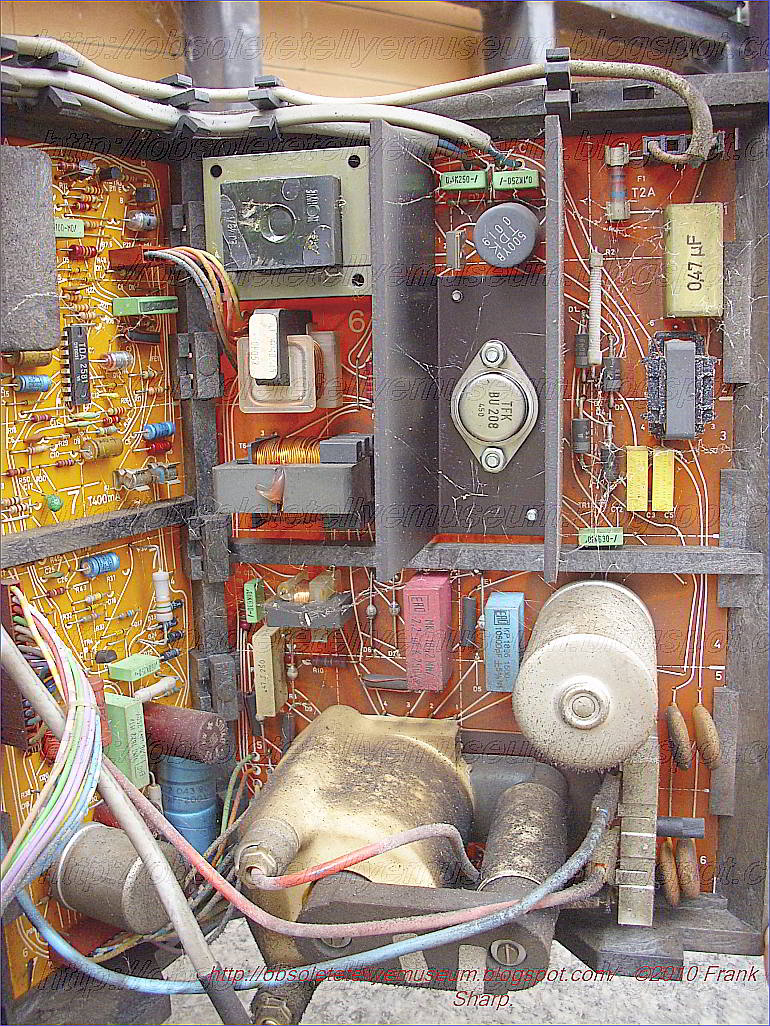


The chassis is an awesome example of enegineering.
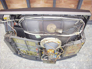
The Beovision 8800 used a chassis that came to be known as the 33XX. This reference came from the type numbers of the sets that used this chassis, most of which started with “33”. The chassis was fully modularised in construction and could be repaired by replacing plug-in units with no soldering being necessary. This design philosophy also allowed upgrades and updates to the design to be made easily as technology changed. One example of this was the receiver panel, which was initially very similar to that of the Beovision 4402 et al but was soon redesigned to take advantage of new integrated circuits and special filters. Another was the colour decoder, which in later sets was revised into an advanced single-chip design.
BANG & OLUFSEN BEOVISION 8800 CHASSIS 3321 30AX Horizontal deflection output circuit:
A horizontal deflection output circuit, such as used in a TV receiver or a display device, includes a series circuit composed of a ringing preventing resistor and a one-way switching element connected in parallel with a linearity correcting coil. That one-way switching element is turned on at the beginning of a horizontal scanning period to feed a current to the ringing preventing resistor but is turned off in the vicinity of a fly-back period to block the flow of the current to the ringing preventing resistor. Thus, the power loss due to the current flowing through the ringing preventing resistor for the fly-back period can be reduced according to the present invention.
1. A horizontal deflection output circuit comprising:
a switching element;
a resonant capacitor connected in parallel with said switching element; and
a first series circuit connected in parallel with said switching element and including a horizontal deflection coil and a linearity correcting coil,
wherein the improvement comprises:
a second series circuit connected in parallel with said linearity correcting coil, said second series circuit comprising load means for damping resonance energy in said first series circuit and current control means for limiting the current flow through said load means to the first half of a horizontal scanning period and including a one-way switching element which turns on for a first half of said horizontal scanning period and turns off for the last half of the horizontal scanning period and for a fly-back pulse period, thereby limiting current flow through said load means to the first half of said horizontal scanning period.
2. A horizontal deflection output circuit according to claim 1, wherein said load means includes a resistor. 3. A horizontal deflection output circuit according to claim 2, wherein a capacitor is connected in parallel with said linearity correcting coil. 4. A horizontal deflection output circuit according to claim 2, wherein said one-way switching element is a diode. 5. A horizontal deflection output circuit according to claim 1, wherein said load means includes: a resistor; and current adjusting means for adjusting the current to flow through said resistor. 6. A horizontal deflection output circuit comprising:
a switching element;
a resonant capacitor connected in parallel with said switching element;
a series circuit connected in parallel with said switching element and including a horizontal deflection coil and a linearity correcting coil; and
a switching element;
a resonant capacitor connected in parallel with said switching element; and
a first series circuit connected in parallel with said switching element and including a horizontal deflection coil and a linearity correcting coil,
wherein the improvement comprises:
a second series circuit connected in parallel with said linearity correcting coil, said second series circuit comprising load means for damping resonance energy in said first series circuit and current control means for limiting the current flow through said load means to the first half of a horizontal scanning period and including a one-way switching element which turns on for a first half of said horizontal scanning period and turns off for the last half of the horizontal scanning period and for a fly-back pulse period, thereby limiting current flow through said load means to the first half of said horizontal scanning period.
2. A horizontal deflection output circuit according to claim 1, wherein said load means includes a resistor. 3. A horizontal deflection output circuit according to claim 2, wherein a capacitor is connected in parallel with said linearity correcting coil. 4. A horizontal deflection output circuit according to claim 2, wherein said one-way switching element is a diode. 5. A horizontal deflection output circuit according to claim 1, wherein said load means includes: a resistor; and current adjusting means for adjusting the current to flow through said resistor. 6. A horizontal deflection output circuit comprising:
a switching element;
a resonant capacitor connected in parallel with said switching element;
a series circuit connected in parallel with said switching element and including a horizontal deflection coil and a linearity correcting coil; and
a series circuit connected in parallel with said linearity correcting coil and including load means and a one-way switching element adapted to be turned on for the front half of a horizontal scanning period, said load means including a resistor and current adjusting means for adjusting the current flow through said resistor, said current adjusting means including a transistor connected in series with said resistor and bias voltage feeding means for feeding a bias voltage to the base of said transistor.
7. A horizontal deflection output circuit according to claim 6, wherein a capacitor is connected in parallel with said linearity correcting coil. 8. A horizontal deflection output circuit according to claim 6, wherein said one-way switching element is turned off at least for a fly-back pulse period. 9. A horizontal deflection output circuit according to claim 6, wherein said one-way switching element is a diode. 10. A horizontal deflection output circuit according to claim 6, wherein said bias voltage feeding means includes resistance voltage-dividing means for dividing the voltage between the two terminals of said linearity correcting coil. 11. A horizontal deflection output circuit according to claim 10, wherein a capacitor is connected in parallel with said linearity correcting coil. 12. A horizontal deflection output circuit according to claim 10, wherein said one-way switching element is turned off at least for a fly-back pulse period. 13. A horizontal deflection output circuit according to claim 10, wherein said one-way switching element is a diode. 14. A horizontal deflection output circuit according to claim 10, wherein said bias voltage feeding means includes a time constant circuit composed of a resistor and a capacitor. 15. A horizontal deflection output circuit according to claim 14, wherein a capacitor is connected in parallel with said linearity correcting coil. 16. A horizontal deflection output circuit according to claim 14, wherein said one-way switching element is a diode. 17. A horizontal deflection output circuit according to claim 14, wherein said one-way switching element is turned off at least for a fly-back pulse period. 18. A horizontal deflection output circuit comprising:
a switching element;
a damper diode connected in parallel with said switching element;
a resonant capacitor connected in parallel with said switching element;
a first series circuit connected in parallel with said switching element and including a horizontal deflection coil and a linearity correcting coil;
a second series circuit connected in parallel with said linearity correcting coil, said second series circuit comprising load means for damping resonance energy in said first series circuit and current control means for limiting the current flow through said load means to the first half of a horizontal scanning period and including a one-way switching element which turns on for the first half of said horizontal scanning period and turns off for the last half of said horizontal scanning period and a fly-back pulse period, thereby limiting current flow through said load means to said first half of said horizontal scanning period;
a choke coil connected with the cathode terminal of said damper diode; and
a d.c. current blocking capacitor connected in series with said horizontal deflection coil.
19. A horizontal deflection output circuit according to claim 18, wherein said choke coil is a fly-back transformer. 20. A horizontal deflection output circuit according to claim 19, wherein said load means includes a resistor. 21. A horizontal deflection output circuit according to claim 20, wherein a capacitor is connected in parallel with said linearity correcting coil. 22. A horizontal deflection output circuit according to claim 20, wherein said one-way switching element is a diode. 23. A horizontal deflection output circuit according to claim 19, wherein said load means includes: a resistor; and current adjusting means for adjusting the current to flow through said resistor. 24. A horizontal deflection output circuit comprising:
a switching element;
a damper diode connected in parallel with said switching element;
a resonant capacitor connected in parallel with said switching element;
a series circuit connected in parallel with said switching element and including a horizontal deflection coil and a linearity correcting coil;
a series circuit connected in parallel with said linearity correcting coil and including load means and a one-way switching element adapted to be turned on for the front half of a horizontal scanning period, said load means including a resistor and current adjusting means for adjusting the current flow through said resistor, said current adjusting means including a transistor connected in series with said resistor and bias voltage feeding means for feeding a bias voltage to the base of said transistor;
a choke coil in the form of a fly-back transformer connected with the cathode terminal of said damper diode; and
a d.c. current blocking capacitor connected in series with said horizontal deflection coil.
25. A horizontal deflection output circuit according to claim 24, wherein said one-way switching element is turned off at least for a fly-back pulse period. 26. A horizontal deflection output circuit according to claim 24, wherein a capacitor is connected in parallel with said linearity correcting coil. 27. A horizontal deflection output circuit according to claim 24, wherein said one-way switching element is a diode. 28. A horizontal deflection output circuit according to claim 24, wherein said bias voltage feeding means includes resistance voltage-dividing means for dividing the voltage between the two terminals of said linearity correcting coil. 29. A horizontal deflection output circuit according to claim 28, wherein said bias voltage feeding means includes a time constant circuit composed of a resistor and a capacitor. 30. A horizontal deflection output circuit according to claim 28, wherein said one-way switching element is turned off at least for a fly-back pulse period. 31. A horizontal deflection output circuit according to claim 28, wherein a capacitor is connected in parallel with said linearity correcting coil. 32. A horizontal deflection output circuit according to claim 28, wherein said one-way switching element is a diode.
Description:
BACKGROUND OF THE INVENTION
The present invention relates to a horizontal deflection output circuit which is to be used with a high resolution display and which has a high horizontal deflection frequency and a high output.
In a conventional TV receiver, a horizontal deflection current having a saw-tooth waveform reaches saturation as it approaches its maximum, causing a problem in that the scanning rate of the electron beam is reduced at the extreme right-hand side, as viewed toward the frame of the display, so that the picture reproduced on the face plate is distorted.
The circuit for solving the above-specified problem to form a symmetrical picture is called a "linearity correcting circuit". In order to correct the linearity of the raster scanned on the face plate, the linearity correcting circuit of the prior art is equipped with a linearity correcting coil which is connected in series with a horizontal deflection coil. That linearity correcting coil is so magnetically biased by means of a permanent magnet that its magnetic saturation characteristics are set differently depending upon the direction of the horizontal deflection current. This horizontal deflection circuit is exemplified by Japanese Patent Laid-Open Nos. 40615/1982, 128949/1981, 124850/1980 and U.S. Pat. No. 3,962,603, as shown schematically in FIGS. 1A and 1B.
As shown in FIG. 1A, the horizontal deflection circuit is composed of an input terminal 1, an output transistor 2, a damper diode 3, a resonant capacitor 4, a horizontal deflection coil 5, a linearity correcting coil 6, an S-shaped correction capacitor 7, a choke coil 8, a supply terminal 9, and a permanent magnet 12 for setting the magnetic bias of the linearity correcting coil 6.
The permanent magnet 12 has its polarity arranged so as to apply a magnetic field in the same direction as that of the magnetic field established in the linearity correcting coil in case a horizontal deflection current IDY flows in the direction of arrow a to the horizontal deflection coil 5.
In case the horizontal deflection current IDY flows in the direction of the arrow a, therefore, the linearity correcting coil 6 is more liable to be magnetically saturated than when the horizontal deflection current IDY flows in the reverse direction.
As a result, the inductance of the linearity correcting coil 6 is least in the vicinity of the maximum of the horizontal deflection current so that this current increases.
Thus, the drop of the scanning rate of the electron beam at the right side of the display frame is corrected. In the display, however, the use of a linearity correcting coil will form longitudinal shading streaks at the left side of the display frame. Those streaks are formed as a result of the fact that a ringing current is established in the horizontal deflection current by the resonance of a resonant circuit which is composed of the inductance of the linearity coil 6 and a stray capacity 17, as shown in FIG. 1B.
In order to solve this problem, the horizontal deflection circuit of the prior art is equipped with a resistor 14 which is connected in parallel with the linearity correcting coil 6. By the provision of that resistor 14, the resonant circuit of the stray capacity and the linearity correcting coil has its Q (i.e., quality) factor dropped to reduce the amplitude of the ringing current.
As the horizontal deflection current has its frequency increased and its output raised in accordance with the fineness in the structure of the display, however, there arises another problem that the power loss at the ringing current preventing resistor is increased.
SUMMARY OF THE INVENTION
An object of the present invention is to provide a horizontal deflection output circuit of high speed and output enabled to reduce such ringing of the horizontal deflection current as will raise a problem, when the horizontal linearity is to be corrected by a linearity correcting coil, without inviting an increase in the loss of the output circuit thereby to eliminate in a more advantageous way the longitudinal streaks which might otherwise be formed in a picture frame.
In order to achieve the above-specified object, the horizontal deflection output circuit according to the present invention has a series circuit connected in parallel with a linearity coil, the series circuit being composed of a resistor and a switching element. The switching element is so controlled that it may be turned on only for a predetermined time period including that for which ringing occurs in the horizontal deflection current.
BANG & OLUFSEN BEOVISION 8800 CHASSIS 3321 30AX Horizontal deflection circuit with a start-up power supply
I n a horizontal deflection circuit, a horizontal oscillator, energized by a supply voltage, develops a horizontal frequency switching signal. A deflection outputs stage is responsive to the switching signal and generates scanning current in a horizontal deflection winding. After commencement of oscillator operation, the voltage developed across a secondary winding of a flyback transformer is rectified and filtered and applied to the horizontal oscillator as the oscillator energizing supply voltage. A start-up supply for developing the oscillator supply voltage during an initial interval includes a source of voltage that is available for use prior to the commencement of oscillator operation, a capacitor, a charging circuit for charging the capacitor from the available voltage source, and a controllable switch coupled to the capacitor and to the oscillator. After the charging circuit has charged the capacitor to a predetermined threshold voltage level, the controllable switch is made conductive to apply the capacitor voltage to the oscillator to commence oscillator operation. The switch is arranged with the capacitor as a relaxation oscillator to begin discharging the capacitor by the load current drawn by the horizontal oscillator. Should the capacitor discharge to a lower threshold level before the flyback-derived supply voltage is developed, the relaxation oscillator changes states to disconnect the horizontal oscillator from the capacitor to initiate a capacitor recharging cycle.
1. An oscillator-derived power supply with start-up circuitry, comprising:
a supply terminal;
an oscillator being energized by the voltage developed at said supply terminal for producing an oscillator output signal;
a start-up voltage supply to energize said oscillator into commencing operation, said start-up voltage supply comprising:
a capacitor,
a source of DC input voltage available prior to commencement of oscillator operation,
means for charging said capacitor from said DC input voltage source, and
switching means interposed between said capacitor and said supply terminal for applying said capacitor voltage to said oscillator after said capacitor has charged to a first threshold level, to commence oscillator operation;
means responsive to said oscillator output signal for developing a steady-state voltage; and
means for applying said steady-state voltage to said supply terminal via said switching means to maintain oscillator energization during steady-state operation.
2. A supply according to claim 1 wherein the minimum load current required by said oscillator to commence operation exceeds in magnitude the current being provided to said capacitor by said charging means.
3. A supply according to claim 2 wherein said capacitor is being discharged to lower voltage by said oscillator after said switching means applies said capacitor voltage to said supply terminal and prior to steady-state oscillator operation.
4. A supply according to claim 3 wherein said steady-state voltage maintains said capacitor charged to a substantially constant voltage level during said steady-state operation.
5. A supply according to claim 4 wherein said DC input voltage is of greater magnitude than the magnitude of said substantially constant voltage level.
6. A supply according to claim 4 wherein said switching means serves to disconnect said capacitor from said supply terminal when said capacitor discharges to a second threshold level lower than said first threshold level to enable said capacitor to recharge.
7. A supply according to claim 6 wherein said steady-state voltage applying means comprises a diode blocking current flow from said charging means to said steady-state voltage developing means.
8. A supply according to any preceding claim wherein said oscillator comprises a deflection generator oscillator and wherein said oscillator output signal responsive means comprises a deflection generator output stage, a flyback transformer coupled to said output stage for developing a flyback pulse voltage across a transformer secondary winding, and rectifying and filtering means for developing said steady-state voltage from said flyback pulse voltage.
 9. A deflection circuit-derived power supply with a start-up supply for the deflection circuit oscillator, comprising:
a horizontal oscillator energized by a supply voltage for developing a horizontal frequency switching signal after commencement of oscillator operation;
a horizontal deflection winding;
a deflection output stage responsive to said horizontal frequency switching signal for generating scanning current in said deflection winding;
a flyback transformer having a first winding coupled to said deflection output stage for developing a horizontal frequency alternating polarity output voltage across a plurality of secondary windings;
supply voltage producing means responsive to the horizontal frequency alternating polarity output voltage developed across one of said plurality of secondary windings for producing said supply voltage after commencement of horizontal oscillator operation; and
a start-up supply for developing said supply voltage during an initial interval to enable said horizontal oscillator to commence operation, said start-up supply comprising:
a source of voltage available prior to commencement of horizontal oscillator operation,
a capacitor,
means for charging said capacitor from said prior available voltage source, and
switching means coupled to said capacitor and to said horizontal oscillator for applying said capacitor voltage to said horizontal oscillator as said supply voltage to commence horizontal oscillator operation after said charging means has charged said capacitor to an upper threshold voltage level, said switching means arranged with said capacitor as a relaxation oscillator that begins discharging said capacitor by the load current drawn by said horizontal oscillator after said charging means has charged said capacitor to said upper threshold voltage level and begins recharging said capacitor from said charging means when said capacitor discharges to a lower threshold voltage level.
BANG & OLUFSEN BEOVISION 8800 CHASSIS 3321 30AX Horizontal deflection circuit with a start-up power supply
I
 n a horizontal deflection circuit, a horizontal oscillator, energized by a supply voltage, develops a horizontal frequency switching signal. A deflection outputs stage is responsive to the switching signal and generates scanning current in a horizontal deflection winding. After commencement of oscillator operation, the voltage developed across a secondary winding of a flyback transformer is rectified and filtered and applied to the horizontal oscillator as the oscillator energizing supply voltage. A start-up supply for developing the oscillator supply voltage during an initial interval includes a source of voltage that is available for use prior to the commencement of oscillator operation, a capacitor, a charging circuit for charging the capacitor from the available voltage source, and a controllable switch coupled to the capacitor and to the oscillator. After the charging circuit has charged the capacitor to a predetermined threshold voltage level, the controllable switch is made conductive to apply the capacitor voltage to the oscillator to commence oscillator operation. The switch is arranged with the capacitor as a relaxation oscillator to begin discharging the capacitor by the load current drawn by the horizontal oscillator. Should the capacitor discharge to a lower threshold level before the flyback-derived supply voltage is developed, the relaxation oscillator changes states to disconnect the horizontal oscillator from the capacitor to initiate a capacitor recharging cycle.
1. An oscillator-derived power supply with start-up circuitry, comprising:
a supply terminal;
an oscillator being energized by the voltage developed at said supply terminal for producing an oscillator output signal;
a start-up voltage supply to energize said oscillator into commencing operation, said start-up voltage supply comprising:
a capacitor,
a source of DC input voltage available prior to commencement of oscillator operation,
means for charging said capacitor from said DC input voltage source, and
switching means interposed between said capacitor and said supply terminal for applying said capacitor voltage to said oscillator after said capacitor has charged to a first threshold level, to commence oscillator operation;
means responsive to said oscillator output signal for developing a steady-state voltage; and
means for applying said steady-state voltage to said supply terminal via said switching means to maintain oscillator energization during steady-state operation.
2. A supply according to claim 1 wherein the minimum load current required by said oscillator to commence operation exceeds in magnitude the current being provided to said capacitor by said charging means.
3. A supply according to claim 2 wherein said capacitor is being discharged to lower voltage by said oscillator after said switching means applies said capacitor voltage to said supply terminal and prior to steady-state oscillator operation.
4. A supply according to claim 3 wherein said steady-state voltage maintains said capacitor charged to a substantially constant voltage level during said steady-state operation.
5. A supply according to claim 4 wherein said DC input voltage is of greater magnitude than the magnitude of said substantially constant voltage level.
6. A supply according to claim 4 wherein said switching means serves to disconnect said capacitor from said supply terminal when said capacitor discharges to a second threshold level lower than said first threshold level to enable said capacitor to recharge.
7. A supply according to claim 6 wherein said steady-state voltage applying means comprises a diode blocking current flow from said charging means to said steady-state voltage developing means.
8. A supply according to any preceding claim wherein said oscillator comprises a deflection generator oscillator and wherein said oscillator output signal responsive means comprises a deflection generator output stage, a flyback transformer coupled to said output stage for developing a flyback pulse voltage across a transformer secondary winding, and rectifying and filtering means for developing said steady-state voltage from said flyback pulse voltage.
a horizontal oscillator energized by a supply voltage for developing a horizontal frequency switching signal after commencement of oscillator operation;
a horizontal deflection winding;
a deflection output stage responsive to said horizontal frequency switching signal for generating scanning current in said deflection winding;
a flyback transformer having a first winding coupled to said deflection output stage for developing a horizontal frequency alternating polarity output voltage across a plurality of secondary windings;
supply voltage producing means responsive to the horizontal frequency alternating polarity output voltage developed across one of said plurality of secondary windings for producing said supply voltage after commencement of horizontal oscillator operation; and
a start-up supply for developing said supply voltage during an initial interval to enable said horizontal oscillator to commence operation, said start-up supply comprising:
a source of voltage available prior to commencement of horizontal oscillator operation,
a capacitor,
means for charging said capacitor from said prior available voltage source, and
switching means coupled to said capacitor and to said horizontal oscillator for applying said capacitor voltage to said horizontal oscillator as said supply voltage to commence horizontal oscillator operation after said charging means has charged said capacitor to an upper threshold voltage level, said switching means arranged with said capacitor as a relaxation oscillator that begins discharging said capacitor by the load current drawn by said horizontal oscillator after said charging means has charged said capacitor to said upper threshold voltage level and begins recharging said capacitor from said charging means when said capacitor discharges to a lower threshold voltage level.

10. A supply according to claim 9 wherein said switching means comprises a first transistor interposed between said capacitor and said horizontal oscillator and a second transistor coupled to said capacitor and to a control electrode of said first transistor.
11. A supply according to claim 9 wherein said supply voltage producing means comprises means for rectifying and filtering said horizontal frequency alternating polarity output voltage and means for applying the output of said rectifying and filtering means to said capacitor to develop said supply voltage as a substantially constant voltage across said capacitor.
12. A supply according to claim 11 wherein said prior available voltage source comprises a source of DC input voltage of magnitude greater than said substantially constant voltage.
Description:
This invention relates to start-up supplies for horizontal deflection circuits.
In a television receiver, the supply voltages to power various television receiver circuits such as the vertical deflection circuit and the audio and video circuits are derived from rectified and filtered flyback pulses developed by the horizontal deflection circuit. After the horizontal oscillator in the deflection circuit has commenced operation, the supply voltage for the oscillator is also derived from rectified and filtered flyback pulse voltages.
When the television receiver is turned on, the flyback pulse voltages are absent. A start-up supply for the horizontal oscillator is therefore required in order to energize the oscillator and develop the flyback-derived power supply voltages for the television receiver. A voltage that is available to power the oscillator during the start-up interval after the television receiver is turned on is the DC input voltage obtained by rectifying and filtering the AC mains supply voltage.
 Since the horizontal oscillator is designed to use a relatively low supply voltage, the DC input voltage during start-up may be applied to the oscillator through a dropping resistor. The value of the resistor is selected to be relatively large in order to minimize the dissipation in the resistor while at the same time providing the horizontal oscillator with at least the minimum amount of current required to initiate oscillator operation. After the flyback-derived supply voltage becomes available, the normal load current for the oscillator is provided from this supply excluding the load current still being provided by the dropping resistor. Thus, the dropping resistor dissipates a significant amount of power even during steady-state television receiver operation after the start-up interval has elapsed.
To eliminate power dissipation in the dropping resistor during steady-state operation, some start-up circuits include a transistor switch in series with the dropping resistor. When the steady-state flyback-derived supply voltage for the oscillator is developed, the switch becomes reverse biased, disconnecting the dropping resistor from the oscillator. A relatively expensive switch is required that is capable of withstanding the off-state voltage stress applied to it. This off-state voltage equals the difference between the DC input voltage and the oscillator supply voltage.
A feature of the invention is the design of an oscillator-derived power supply with start-up circuitry that dissipates relatively little power during steady-state operation after the oscillator has commenced operation. An oscillator energized by the voltage developed at a supply terminal produces an output signal that is used by a subsequent power supply stage to develop a steady-state voltage to energize the load circuit. The steady-state voltage is also applied to the oscillator to maintain it energized after commencement of oscillator operation. A start-up voltage supply to energize the oscillator into commencing operation comprises a capacitor, a source of energy that is available prior to the commencement of oscillator operation, a charging circuit for charging the capacitor from the energy source, and switching means interposed between the capacitor and the oscillator. The switching means applies the capacitor voltage to the oscillator after the capacitor has charged to a first threshold level, thereby commencing oscillator operation and the development of the steady-state voltage by the oscillator responsive power supply.
With such an arrangement, the charging current flowing to the capacitor may be selected to be of relatively low magnitude, much lower than even the minimum amount of load current required to energize the oscillator. Dissipation in the charging circuit is substantially reduced, even though the charging circuit may still be supplying current during steady-state operation after commencement of oscillator operation.
 During the start-up interval, the oscillator draws more current from the capacitor than is being supplied by the charging circuit, resulting in the capacitor being discharged. Another feature of the invention is that should the capacitor discharge to a lower threshold level, indicating that the steady-state voltage supply is still unavailable for use, the switching means disconnects the capacitor from the oscillator, enabling the capacitor to recharge and reinitiate the start-up sequence.
FIG. 1 illustrates a horizontal deflection circuit with derived power supplies and with a start-up circuit for the deflection oscillator; and
FIG. 2 illustrates waveforms associated with the circuit of FIG. 1.
In FIG. 1, a source 20 of AC mains supply voltage is coupled to input terminals 23 and 24 of a full-wave bridge rectifier 27. Source 20 is coupled to input terminal 23 through an on/off switch 21 and a current limiting resistor 22. A filter capacitor 28 is coupled across output terminal 25 of bridge rectifier 27 and the current return or ground terminal 26. A filtered but unregulated DC input voltage Vin is developed at terminal 25 and applied to a regulator 29. Regulator 29 may be a conventional switching regulator, such as described in U.S. Pat. No. 4,147,964, D. W. Luz et al., entitled "COMPLEMENTARY LATCHING DISABLING CIRCUIT", using an SCR regulator switch operated at the horizontal deflection frequency of a television receiver to produce a regulated B+ voltage at a terminal 30. Feedback of the B+ voltage to the switching regulator is provided by a conductor line 74. A filter capacitor 31 is provided to filter out horizontal rate ripple voltage from terminal 30.
The B+ voltage developed at terminal 30 is applied through the primary winding 32a of a flyback transformer 32 to the collector of a horizontal output transistor 35 in a horizontal deflection output stage 34 of a horizontal deflection circuit 80. Horizontal deflection circuit 80 includes a horizontal oscillator 43, energized by a supply voltage Vcc developed at a supply terminal 45 and drawing a load current iL therefrom, a horizontal driver transistor 44 and horizontal output stage 34. Horizontal output stage 34 comprises horizontal output transistor 35, a damper diode 36, a retrace capacitor 38 and the series arrangement of a horizontal deflection winding 39 and an S-shaping or trace capacitor 40.
 Horizontal oscillator 43, when energized by the voltage developed at supply terminal 45, produces a horizontal frequency, 1/TH, output switching signal 37 that is inverted by horizontal driver transistor 44 and applied to horizontal output transistor 35 through a driver transformer 42 to produce the switching action needed to generate horizontal scanning current in horizontal deflection winding 39. A waveshaping and filtering network 41 is coupled between the secondary winding 42b of driver transformer 42 and the base and emitter electrodes of output transistor 35.
Horizontal output transistor 35 is turned on early within the trace interval of each deflection cycle to conduct the horizontal scanning current after damper diode 36 is cut off and is turned off to initiate the horizontal retrace interval. During horizontal retrace, a retrace pulse voltage Vr is developed at the collector of horizontal output transistor 35 and applied to flyback transformer primary winding 32a to develop alternating polarity horizontal retrace pulse voltages across secondary windings 32b-32d.
 The high voltage developed across winding 32b is applied to a high voltage circuit 33 to develop a DC ultor accelerating potential at a terminal U. The voltage across flyback transformer secondary winding 32c is rectified by a diode 46 during the horizontal trace interval and filtered by a capacitor 47 to develop a DC supply voltage V1 at a terminal 49. Supply voltage V1 energizes and provides current to such television receiver load circuits as the vertical deflection circuit and the audio circuit, designated in FIG. 1 generally as a resistor 48. The voltage across flyback transformer secondary winding 32d is rectified during the horizontal retrace interval by a diode 51 and applied to a supply terminal 53 through a current limiting resistor 52 to develop a DC supply voltage V2 across a filter capacitor 54. The DC supply voltage V2 energizes and provides current to such television receiver load circuits as the video driver circuit designated in FIG. 1 generally as a resistor 55.
The rectified and filtered voltage from flyback transformer winding 32d also supplies the collector voltage for horizontal driver transistor 44. The substantially DC voltage developed at the cathode of diode 51 at terminal 50 is applied through a resistor 57 and primary winding 42a of driver transformer 42 to the collector of driver transistor 44. A capacitor 56 provides horizontal rate filtering.
When the television receiver is turned on, after closure of on/off switch 21, the unregulated DC input voltage Vin is developed at terminal 25 and applied to switching regulator 29 to develop a voltage at B+ terminal 30. During the initial or start-up interval following closure of on/off switch 21, the flyback-derived supply voltages V1 and V2 are absent. To generate these voltages, switching action of horizontal output transistor 35 must be initiated by initiating or commencing the switching actions of horizontal oscillator 43 and driver transistor 44. Energization of these two elements, 43 and 44, must be obtained from voltage or energy sources that are available for use prior to commencement of operation of horizontal oscillator 43 and driver transistor 44.
The voltage used during start-up for providing collector supply voltage to driver transistor 44 is the voltage developed at B+ terminal 30 after closure of on/off switch 21. Terminal 30 is coupled to terminal 50 through a resistor 59 and a diode 60. Collector voltage for driver transistor 44 is obtained from B+ terminal 30 during start-up by way of resistor 59 and diode 60.
A start-up supply 90 is provided to initially develop supply voltage for horizontal oscillator 43 to energize the oscillator into commencing operation. Start-up supply 90 comprises a capacitor 63, a transistor switch 66 interposed between capacitor 63 and horizontal oscillator 43 at the supply terminal 45, a source of energy or voltage available prior to commencement of oscillator operation, namely the source of the DC input voltage Vin, and a charging resistor 61 that is used to charge capacitor 63 during the start-up interval from the DC input voltage terminal 25 by way of a resistor 62. Resistor 62 is a relatively low valued resistor used for a purpose hereinafter to be described.
Upon closureof on/off switch 21 and the development of a DC voltage Vin at terminal 25, a charging current ic begins to flow through resistor 61 and resistor 62 to terminal 73, the junction of capacitor 63 and the emitter of controllable transistor switch 66. Capacitor 63 is initially uncharged and the voltage Vc at terminal 73 is zero, maintaining transistor switch 66 in the off-state immediately after closure of on/off switch 21.
The base of transistor switch 66 is coupled to the collector of a transistor 67 through a resistor 72. A biasing network for transistors 66 and 67, comprising resistors 68-72, establishes at terminal 73 an upper threshold voltage level Va and a lower threshold voltage level Vb so as to enable transistors 66 and 67 to form with capacitor 63 a relaxation oscillator arrangement. When transistor 66 is cut off, resistor 70 is effectively in parallel with resistor 69, thereby establishing the upper threshold voltage level Va of FIG. 2; and when transistor 66 is in saturated conduction, resistor 70 is effectively in parallel with resistor 68, thereby establishing the lower threshold voltage level Vb.
As illustrated in FIG. 2 by the solid-line waveform of the voltage Vc, at a time t0, on/off switch 21 is closed and the charging current ic flowing from terminal 73 begins to charge capacitor 63. At time t1, capacitor 63 has charged to the upper threshold voltage level Va, turning on transistor 67 which turns on transistor switch 66 into saturated conduction. After transistor 66 becomes conductive, the voltage across capacitor 63 is applied to horizontal oscillator 43 at supply terminal 45 as a start-up supply voltage for the horizontal oscillator. Horizontal oscillator 43 commences operation and begins producing the horizontal rate switching signal 37 to initiate the switching action of horizontal driver transistor 44 and horizontal output transistor 35, thereby initiating the development of the horizontal retrace pulse voltage Vr and the horizontal retrace pulse voltages across flyback transformer secondary windings 32b-32d.
The load current iL being drawn by horizontal oscillator 43 durin g the initial or start-up interval, after time t1 of FIG. 2, is of greater magnitude than the charging current ic flowing to terminal 73 from charging resistor 61. Thus, after time t1, horizontal oscillator 43 begins discharging capacitor 63 as illustrated in FIG. 2 by the decreasing voltage Vc after time t1. Even though the voltage Vc applied to horizontal oscillator 43 during the start-up interval after time t1 is decreasing, it is still sufficiently greater than the minimum voltage needed to maintain the oscillator operating. Thus, the horizontal rate switching signal is still being produced by horizontal oscillator 43 after time t1. By time t2 of FIG. 2, a sufficient period has elapsed so as to enable a substantial buildup of the flyback-derived supply voltage V1 at terminal 49. Supply voltage V1 is then applied to horizontal oscillator 43 by way of a diode 64 that has its cathode coupled to terminal 65, the junction of charging resistor 61 and resistor 62. Diode 64 blocks the flow of charging current to flyback supply terminal to prevent undue shunting of the current from oscillator 43 during start-up.
Near time t2, the flyback-derived supply voltage V1 has increased sufficiently so as to be able to generate a current i1 flowing out of supply terminal 49 that is greater than the load current iL being drawn by horizontal oscillator 43. Thus, after time t2, capacitor 63 ceases discharging and becomes charged shortly thereafter to a relatively constant voltage level Vcc0, as illustrated by the solid-line waveform of FIG. 2 after time t2.
The voltage Vcc0 maintains transistor switch 66 conducting and is applied via the transistor to horizontal oscillator 43 as the steady-state supply voltage. Thus, the steady-state supply voltage Vcc0 is obtained from the flyback-derived supply voltage V1. Because the flyback-derived supply voltage V1 also functions as a supply voltage for other television receiver loads, the voltage V1 is not necessarily of the ideal magnitude to energize horizontal oscillator 43. Typically, the voltage V1 is slightly greater in magnitude than is desirable for use by horizontal oscillator 43. Resistor 62 is therefore provided to generate a voltage drop to establish the correct lower voltage Vcc0 at supply terminal 45.
During steady-state operation, the load current iL for horizontal oscillator 43 comprises the sum of the current i1 obtained from flyback supply terminal 49 and the charging current ic obtained from charging resistor 61, if the biasing currents to transistors 66 and 67 are neglected. Thus, even during steady-state operation, the charging current ic flows through resistor 61.
To keep power dissipation in charging resistor 61 to a relatively small amount especially during steady-state operation, the magnitude of the charging current ic is kept at a relatively small value, illustratively at 5% or less of the steady-state load current of horizontal oscillator 43 and 10 times less than the minimum load current needed to maintain horizontal oscillator 43 operating at start-up. By providing a transistor 66 interposed between capacitor 63 and oscillator supply terminal 45, the current required to flow through the resistance that is coupled between the DC input voltage Vin and oscillator 43 may be kept relatively small to reduce steady-state dissipation. Sufficient start-up load current to horizontal oscillator 43 is available, nonetheless, due to the charge buildup on capacitor 63 and the subsequent discharge of the capacitor.
The values of the upper threshold voltage level Va and of the capacitance of capacitor 63 may be selected such that for almost every deflection circuit operating condition encountered, sufficient time is available after capacitor 63 begins to be discharged by the load current drawn by horizontal oscillator 43 to enable the flyback-derived supply voltage V1 to subsequently take over energization of the oscillator before the capacitor has discharged to a voltage less than the minimum required to maintain operation of the oscillator.
Another feature of the invention is to arrange transistor switch 66, transistor 67 and capacitor 63 as a relaxation oscillator. By providing a relaxation oscillator arrangement, start-up of horizontal deflection circuit 80 is ensured for practically all operating conditions encountered by horizontal deflection circuit 80. For example, a situation may be encountered during start-up where the DC input voltage Vin is extremely low and the loading on flyback transformer 32 is extremely high. In such an operating situation, a much longer interval after the initiation of start-up may be required to build up the flyback-derived supply voltage V1 to a satisfactory level. If capacitor 63 discharges to a level below the minimum necessary to maintain horizontal oscillator 43 in operation before the voltage V1 builds up to a satisfactory level, start-up of deflection circuit 80 is defeated.
To prevent such a situation from occurring, the relaxation oscillator arrangement of start-up supply 90 establishes a lower threshold voltage level Vb when transistor switch 66 is conductive. Should capacitor 63 discharge to the lower threshold voltage level Vb, as illustrated by FIG. 2 by the dashed-line waveform of the voltage Vc after time t2, indicating a failure of the flyback-derived supply voltage V1 to build up to a satisfactory level, transistor 67 is biased off, thereby turning off transistor switch 66. The value of the lower threshold voltage level Vb may be selected as greater than the minimum voltage needed to maintain oscillator 43 functioning.
In a television receiver, the supply voltages to power various television receiver circuits such as the vertical deflection circuit and the audio and video circuits are derived from rectified and filtered flyback pulses developed by the horizontal deflection circuit. After the horizontal oscillator in the deflection circuit has commenced operation, the supply voltage for the oscillator is also derived from rectified and filtered flyback pulse voltages.
When the television receiver is turned on, the flyback pulse voltages are absent. A start-up supply for the horizontal oscillator is therefore required in order to energize the oscillator and develop the flyback-derived power supply voltages for the television receiver. A voltage that is available to power the oscillator during the start-up interval after the television receiver is turned on is the DC input voltage obtained by rectifying and filtering the AC mains supply voltage.

To eliminate power dissipation in the dropping resistor during steady-state operation, some start-up circuits include a transistor switch in series with the dropping resistor. When the steady-state flyback-derived supply voltage for the oscillator is developed, the switch becomes reverse biased, disconnecting the dropping resistor from the oscillator. A relatively expensive switch is required that is capable of withstanding the off-state voltage stress applied to it. This off-state voltage equals the difference between the DC input voltage and the oscillator supply voltage.
A feature of the invention is the design of an oscillator-derived power supply with start-up circuitry that dissipates relatively little power during steady-state operation after the oscillator has commenced operation. An oscillator energized by the voltage developed at a supply terminal produces an output signal that is used by a subsequent power supply stage to develop a steady-state voltage to energize the load circuit. The steady-state voltage is also applied to the oscillator to maintain it energized after commencement of oscillator operation. A start-up voltage supply to energize the oscillator into commencing operation comprises a capacitor, a source of energy that is available prior to the commencement of oscillator operation, a charging circuit for charging the capacitor from the energy source, and switching means interposed between the capacitor and the oscillator. The switching means applies the capacitor voltage to the oscillator after the capacitor has charged to a first threshold level, thereby commencing oscillator operation and the development of the steady-state voltage by the oscillator responsive power supply.
With such an arrangement, the charging current flowing to the capacitor may be selected to be of relatively low magnitude, much lower than even the minimum amount of load current required to energize the oscillator. Dissipation in the charging circuit is substantially reduced, even though the charging circuit may still be supplying current during steady-state operation after commencement of oscillator operation.
FIG. 1 illustrates a horizontal deflection circuit with derived power supplies and with a start-up circuit for the deflection oscillator; and
FIG. 2 illustrates waveforms associated with the circuit of FIG. 1.
In FIG. 1, a source 20 of AC mains supply voltage is coupled to input terminals 23 and 24 of a full-wave bridge rectifier 27. Source 20 is coupled to input terminal 23 through an on/off switch 21 and a current limiting resistor 22. A filter capacitor 28 is coupled across output terminal 25 of bridge rectifier 27 and the current return or ground terminal 26. A filtered but unregulated DC input voltage Vin is developed at terminal 25 and applied to a regulator 29. Regulator 29 may be a conventional switching regulator, such as described
in U.S. Pat. No. 4,147,964, D. W. Luz et al., entitled "COMPLEMENTARY LATCHING DISABLING CIRCUIT", using an SCR regulator switch operated at the horizontal deflection frequency of a television receiver to produce a regulated B+ voltage at a terminal 30. Feedback of the B+ voltage to the switching regulator is provided by a conductor line 74. A filter capacitor 31 is provided to filter out horizontal rate ripple voltage from terminal 30.The B+ voltage developed at terminal 30 is applied through the primary winding 32a of a flyback transformer 32 to the collector of a horizontal output transistor 35 in a horizontal deflection output stage 34 of a horizontal deflection circuit 80. Horizontal deflection circuit 80 includes a horizontal oscillator 43, energized by a supply voltage Vcc developed at a supply terminal 45 and drawing a load current iL therefrom, a horizontal driver transistor 44 and horizontal output stage 34. Horizontal output stage 34 comprises horizontal output transistor 35, a damper diode 36, a retrace capacitor 38 and the series arrangement of a horizontal deflection winding 39 and an S-shaping or trace capacitor 40.
Horizontal output transistor 35 is turned on early within the trace interval of each deflection cycle to conduct the horizontal scanning current after damper diode 36 is cut off and is turned off to initiate the horizontal retrace interval. During horizontal retrace, a retrace pulse voltage Vr is developed at the collector of horizontal output transistor 35 and applied to flyback transformer primary winding 32a to develop alternating polarity horizontal retrace pulse voltages across secondary windings 32b-32d.
The rectified and filtered voltage from flyback transformer winding 32d also supplies the collector voltage for horizontal driver transistor 44. The substantially DC voltage developed at the cathode of diode 51 at terminal 50 is applied through a resistor 57 and primary winding 42a of driver transformer 42 to the collector of driver transistor 44. A capacitor 56 provides horizontal rate filtering.
When the television receiver is turned on, after closure of on/off switch 21, the unregulated DC input voltage Vin is developed at terminal 25 and applied to switching regulator 29 to develop a voltage at B+ terminal 30. During the initial or start-up interval following closure of on/off switch 21, the flyback-derived supply voltages V1 and V2 are absent. To generate these voltages, switching action of horizontal output transistor 35 must be initiated by initiating or commencing the switching actions of horizontal oscillator 43 and driver transistor 44. Energization of these two elements, 43 and 44, must be obtained from voltage or energy sources that are available for use prior to commencement of operation of horizontal oscillator 43 and driver transistor 44.
The voltage used during start-up for providing collector supply voltage to driver transistor 44 is the voltage developed at B+ terminal 30 after closure of on/off switch 21. Terminal 30 is coupled to terminal 50 through a resistor 59 and a diode 60. Collector voltage for driver transistor 44 is obtained from B+ terminal 30 during start-up by way of resistor 59 and diode 60.
A start-up supply 90 is provided to initially develop supply voltage for horizontal oscillator 43 to energize the oscillator into commencing operation. Start-up supply 90 comprises a capacitor 63, a transistor switch 66 interposed between capacitor 63 and horizontal oscillator 43 at the supply terminal 45, a source of energy or voltage available prior to commencement of oscillator operation, namely the source of the DC input voltage Vin, and a charging resistor 61 that is used to charge capacitor 63 during the start-up interval from the DC input voltage terminal 25 by way of a resistor 62. Resistor 62 is a relatively low valued resistor used for a purpose hereinafter to be described.
Upon closure
of on/off switch 21 and the development of a DC voltage Vin at terminal 25, a charging current ic begins to flow through resistor 61 and resistor 62 to terminal 73, the junction of capacitor 63 and the emitter of controllable transistor switch 66. Capacitor 63 is initially uncharged and the voltage Vc at terminal 73 is zero, maintaining transistor switch 66 in the off-state immediately after closure of on/off switch 21.The base of transistor switch 66 is coupled to the collector of a transistor 67 through a resistor 72. A biasing network for transistors 66 and 67, comprising resistors 68-72, establishes at terminal 73 an upper threshold voltage level Va and a lower threshold voltage level Vb so as to enable transistors 66 and 67 to form with capacitor 63 a relaxation oscillator arrangement. When transistor 66 is cut off, resistor 70 is effectively in parallel with resistor 69, thereby establishing the upper threshold voltage level Va of FIG. 2; and when transistor 66 is in saturated conduction, resistor 70 is effectively in parallel with resistor 68, thereby establishing the lower threshold voltage level Vb.
As illustrated in FIG. 2 by the solid-line waveform of the voltage Vc, at a time t0, on/off switch 21 is closed and the charging current ic flowing from terminal 73 begins to charge capacitor 63. At time t1, capacitor 63 has charged to the upper threshold voltage level Va, turning on transistor 67 which turns on transistor switch 66 into saturated conduction. After transistor 66 becomes conductive, the voltage across capacitor 63 is applied to horizontal oscillator 43 at supply terminal 45 as a start-up supply voltage for the horizontal oscillator. Horizontal oscillator 43 commences operation and begins producing the horizontal rate switching signal 37 to initiate the switching action of horizontal driver transistor 44 and horizontal output transistor 35, thereby initiating the development of the horizontal retrace pulse voltage Vr and the horizontal retrace pulse voltages across flyback transformer secondary windings 32b-32d.
The load current iL being drawn by horizontal oscillator 43 durin
 g the initial or start-up interval, after time t1 of FIG. 2, is of greater magnitude than the charging current ic flowing to terminal 73 from charging resistor 61. Thus, after time t1, horizontal oscillator 43 begins discharging capacitor 63 as illustrated in FIG. 2 by the decreasing voltage Vc after time t1. Even though the voltage Vc applied to horizontal oscillator 43 during the start-up interval after time t1 is decreasing, it is still sufficiently greater than the minimum voltage needed to maintain the oscillator operating. Thus, the horizontal rate switching signal is still being produced by horizontal oscillator 43 after time t1. By time t2 of FIG. 2, a sufficient period has elapsed so as to enable a substantial buildup of the flyback-derived supply voltage V1 at terminal 49. Supply voltage V1 is then applied to horizontal oscillator 43 by way of a diode 64 that has its cathode coupled to terminal 65, the junction of charging resistor 61 and resistor 62. Diode 64 blocks the flow of charging current to flyback supply terminal to prevent undue shunting of the current from oscillator 43 during start-up.
Near time t2, the flyback-derived supply voltage V1 has increased sufficiently so as to be able to generate a current i1 flowing out of supply terminal 49 that is greater than the load current iL being drawn by horizontal oscillator 43. Thus, after time t2, capacitor 63 ceases discharging and becomes charged shortly thereafter to a relatively constant voltage level Vcc0, as illustrated by the solid-line waveform of FIG. 2 after time t2.
During steady-state operation, the load current iL for horizontal oscillator 43 comprises the sum of the current i1 obtained from flyback supply terminal 49 and the charging current ic obtained from charging resistor 61, if the biasing currents to transistors 66 and 67 are neglected. Thus, even during steady-state operation, the charging current ic flows through resistor 61.
The values of the upper threshold voltage level Va and of the capacitance of capacitor 63 may be selected such that for almost every deflection circuit operating condition encountered, sufficient time is available after capacitor 63 begins to be discharged by the load current drawn by horizontal oscillator 43 to enable the flyback-derived supply voltage V1 to subsequently take over energization of the oscillator before the capacitor has discharged to a voltage less than the minimum required to maintain operation of the oscillator.
To prevent such a situation from occurring, the relaxation oscillator arrangement of start-up supply 90 establishes a lower threshold voltage level Vb when transistor switch 66 is conductive. Should capacitor 63 discharge to the lower threshold voltage level Vb, as illustrated by FIG. 2 by the dashed-line waveform of the voltage Vc after time t2, indicating a failure of the flyback-derived supply voltage V1 to build up to a satisfactory level, transistor 67 is biased off, thereby turning off transistor switch 66. The value of the lower threshold voltage level Vb may be selected as greater than the minimum voltage needed to maintain oscillator 43 functioning.
With transistor switch 66 cut off at time t3, a start-up charging cycle for capacitor 63 is reinitiated. As illustrated in FIG. 2 by the dashed-line waveform, capacitor 63 recharges from time t3 to time t4, at which time the upper threshold voltage level Va is again reached at terminal 73 to turn on transistor switch 66 at time t4. The voltage across capacitor 63 is again applied to horizontal oscillator 43 to recommence oscillator operation and to continue the buildup of flyback-derived supply voltage V1 so that by time t5 the supply voltage V1 has increased sufficiently to take over supplying current to horizontal oscillator 43. Shortly after time t5, the steady-state supply voltage Vcc0 at supply terminal 45 is established.
The relaxation oscillator arrangement of start-up supply 90 can provide as many charge/discharge cycles for capacitor 63 as may be required in order to build up the flyback-derived supply voltage V1 to the levels needed to maintain steady-state deflection circuit operation. BANG & OLUFSEN BEOVISION 8800 CHASSIS 3321 30AX CIRCUIT ARRANGEMENT IN A PICTURE DISPLAY DEVICE UTILIZING A STABILIZED SUPPLY VOLTAGE CIRCUIT:TDA2581 CONTROL CIRCUIT FOR SMPS/PHILIPS POWER PACK:
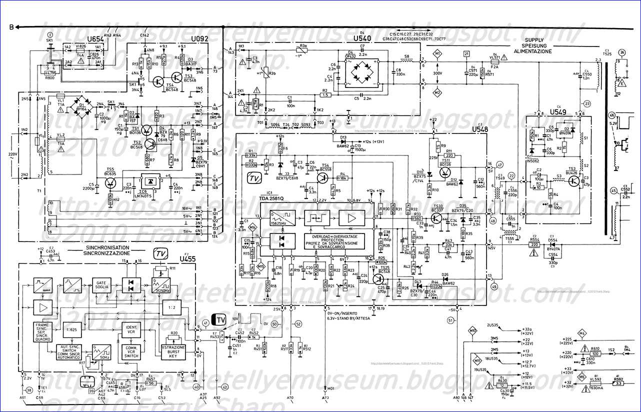
The TDA2581 is a monolithic integrated circuit for controlling switched-mode power supplies (SMPS) which are provided with the drive for the horizontal deflection stage.
The circuit features the following:
— Voltage controlled horizontal oscillator.
— Phase detector.
— Duty factor control for the positive-going transient of the output signal.
— Duty factor increases from zero to its normal operation value.
— Adjustable maximum duty factor.
- Over-voltage and over-current protection with automatic re-start after switch-off.
— Counting circuit for permanent switch-off when n~times over~current or over-voltage is sensed

-Protection for open-reference voltage.
- Protection for too low supply voltage.
Protection against loop faults.
Positive tracking of duty factor and feedback voltage when the feedback voltage is smaller than the
reference voltage minus 1,5 V.
BANG & OLUFSEN BEOVISION 8800 CHASSIS 3321 30AX Line synch Switched Mode Power Supply with Line deflection output Transistor Drive Circuit:
A stabilized supply voltage circuit for a picture display device comprising a chopper wherein the switching signal has the line frequency and is duration-modulated. The coil of the chopper constitutes the primary winding of a transformer a secondary winding of which drives the line output transistor so that the switching transistor of the chopper also functions as a driver for the line output stage. The oscillator generating the switching signal may be the line oscillator. In a special embodiment the driver and line output transistor conduct simultaneously and in order to limit the base current of the line output transistor a coil shunted by a diode is incorporated in the drive line of the line output transistor. Other secondary windings of the transformer drive diodes which conduct simultaneously with the efficiency diode of the chopper so as to generate further stabilized supply voltages.

Description:
The pulse duration modulation is effected by means of a comparison circuit which compares the direct voltage to be stabilized with a substantially constant voltage, the coil constituting the primary winding of a transformer.
voltage device.
It is to be noted that the chopper need not necessarily be formed as that in the mentioned German "Auslegeschrift." In fact, it is known from literature that the efficiency diode and the coil may be exchanged. It is alternatively possible for the coil to be provided at the first terminal of the input voltage whilst the switching transistor is arranged between the other end and the second terminal of the input voltage. The efficiency diode is then provided between the junction of said end and the switching transistor and the load. It may be recognized that for all these modifications a voltage is present across the connections of the coil which voltage has the same frequency and the same shape as the pulsatory switching voltage. The control voltage of a line deflection circuit is a pulsatory voltage which causes the line output transistor to be saturates and cut off alternately. The invention is based on the recognition that the voltage present across the connections of the coil is suitable to function as such a control voltage and that the coil constitutes the primary of a transformer. To this end the circuit arrangement according to the invention is characterized in that a secondary winding of the transformer drives the switching element which applies a line deflection current to line deflection coils and by which the voltage for the final anode of a picture display tube which forms part of the picture display device is generated, and that the ratio between the period during which the switching transistor is saturated and the entire period, i.e., the switching transistor duty cycle is between 0.3 and 0.7 during normal operation.
The invention is also based on the recognition that the duration modulation which is necessary to stabilize the supply voltage with the switching transistor does not exert influence on the driving of the line output transistor. This resides in the fact that in case of a longer or shorter cut-off period of the line output transistor the current flowing through the line deflection coils thereof is not influenced because of the efficiency diode current and transistor current are taken over or, in case of a special kind of transistor, the collector-emitter current is taken over by the base collector current and conversely. However, in that case the above-mentioned ratios of 0.3 : 0.7 should be taken into account since otherwise this take-over principle is jeopardized.
As will be further explained the use of the switching transistor as a driver for the line output transistor in an embodiment to be especially described hereinafter has the further advantage that the line output transistor automatically becomes non-conductive when this switching transistor is short circuited so that the deflection and the EHT for the display tube drop out and thus avoid damage thereof.
Due to the step according to the invention the switching transistor in the stabilized supply functions as a driver for the line deflection circuit. The circuit arrangement according to the invention may in addition be equipped with a very efficient safety circuit so that the reliability is considerably enhanced, which is described in the U.S. Pat. No. 3,629,686. The invention is
In order that the invention may be readily carried into effect, a few embodiments thereof will now be described in detail by way of example with reference to the accompanying diagrammatic drawings in which:
FIG. 1 shows a principle circuit diagram wherein the chopper and the line deflection circuit are further shown but other circuits are not further shown.
FIGS. 2a, 2b and 2c show the variation as a function of time of two currents and of a voltage occurring in the circuit arrangement according to FIG. 1.
FIGS. 3a 3b, 3c and 3d show other embodiments of the chopper.
FIGS. 4a and 4b show modifications of part of the circuit arrangement of FIG. 1.
 In FIG. 1 the reference numeral 1 denotes a rectifier circuit which converts the mains voltage supplied thereto into a non-stabilized direct voltage. The collector of a switching transistor 2 is connected to one of the two terminals between which this direct voltage is obtained, said transistor being of the npn-type in this embodiment and the base of which receives a pulsatory voltage which originates through a control stage 4 from a modulator 5 and causes transistor 2 to be saturated and cut off alternately. The voltage waveform 3 is produced at the emitter of transistor 2. In order to maintain the output voltage of the circuit arrangement constant, the duration of the pulses provided is varied in modulator 5. A pulse oscillator 6 supplies the pulsatory voltage to modulator 5 and is synchronized by a signal of line frequency which originates from the line oscillator 6' present in the picture display device. This line oscillator 6' is in turn directly synchronized in known manner by pulses 7' of line frequency which are present in the device and originate for example from a received television signal if the picture display device is a television receiver. Pulse oscillator 6 thus generates a pulsatory voltage the repetition frequency of which is the line frequency.
The emitter of switching transistor 2 is connected at one end to the cathode of an efficiency diode 7 whose other end is connected to the second input voltage terminal and at the other end to primary winding 8 of a transformer 9. Pulsatory voltage 3 which is produced at the cathode of efficiency diode 7 is clamped against the potential of said second terminal during the intervals when this diode conducts. During the other intervals the pulsatory voltage 3 assumes the value V i . A charge capacitor 10 and a load 11 are arranged between the other end of winding 8 and the second input voltage terminal.
V o = V i . δ
However, variations in the line amplitude and the EHT may occur as a result of an insufficiently small internal impedance of the EHT generator. Compensation means are known for this purpose. A possibility within the scope of the present invention is to use comparison circuit 12 for this purpose. In fact, if the beam current passes through an element having a substantially quadratic characteristic, for example, a voltage-dependent resistor, then a variation for voltage V o may be obtained through comparison circuit 12 which variation is proportional to the root of the variation in the EHT which is a known condition for the line amplitude to remain constant.
It is to be noted that a parabola voltage of line frequency as shown at 28 is produced across the charge capacitor 10 if this capacitor is given a smaller capacitance so that consequently the so-called S-correction is established.
In FIG. 1 charge capacitors are arranged between terminals 15 etc. and earth so as to ensure that the voltages on these points are stabilized direct voltages. If in addition the mean value of the voltage on one of these terminals has been made equal to the effective value of the alternating voltage which is required for heating the filament of the picture display tube present in the picture display device, this voltage is suitable for this heating. This is a further advantage of the invention since the cheap generation of a stabilized filament voltage for the picture display tube has always been a difficult problem in transistorized arrangements.
A further advantage of the picture display device according to the invention is that transformer 9 can function as a separation transformer so that the different secondary windings can be separated from the mains and their lower ends can be connected to ground of the picture display device. The latter step makes it possible to connect a different apparatus such as, for example, a magnetic recording and/or playback apparatus to the picture display device without earth connection problems occurring.
It will now be shown that secondary winding 14 can indeed drive a line deflection circuit so that switching transistor 2 can function as a driver for the line deflection. FIGS. 2a and b show the variation as a function of time of the current i C which flows in the collector of transistor 16 and of the drive voltage v 14 across the terminals of secondary winding 14. During the flyback period (0, t 1 ) transistor 16 must be fully cut off because a high voltage peak is then produced at its collector; voltage v 14 must then be absolutely negative. During the scan period (t 1 , t 4 ) a sawtooth current i C flows through the collector electrode of transistor 16 which current is first negative and then changes its direction. As the circuit arrangement is not free from loss, the instant t 3 when current i C becomes zero lies, as is known, before the middle of the scan period. At the end t 4 of the scan period transistor 16 must be switched off again. However, since transistor 16 is saturated during the scan period and since this transistor must be suitable for high voltages and great powers so that its collector layer is thick, this transistor has a very great excess of charge carriers in both its base and collector layers. The removal of these charge carriers takes a period t s which is not negligible whereafter the transistor is indeed switched off. Thus the fraction δ T of the line period T at which v 14 is positive must end at the latest at the instant (t 4 - t s ) located after the commencement (t = 0) of the previous flyback.
The time δ T may be initiated at any instant t 2 which is located between the end t 1 of the flyback period and the instant t 3 when collector current i C reverses its direction. It is true that emitter current flows through transistor 16 at the instant t 2 , but collector current i C is not influenced thereby, at least not when the supply voltage (= V o ) for line deflection circuit 17 is high enough. All this has been described in the U.S. Pat. No. 3,504,224. The same applies to line deflection circuits wherein the collector base diode does not function as an efficiency diode as is the case in the described circuit 17, but wherein an efficiency diode is arranged between collector and emitter of the line output transistor. In such a case the negative part of the current i C of FIG. 2a represents the current flowing through the said efficiency diode.
After the instant t 3 voltage v 14 must be positive. In other words, the minimum duration of the period T when voltage v 14 must be positive is (t 4 - t s ) - t 3 whilst the maximum duration thereof is (t 4 - t s ) - t 1 . In a television system employing 625 lines per raster the line period t 4 is approximately 64 μus and the flyback period is approximately 12 μus. Without losses in the circuit arrangement instant t 3 would be located approximately 26 μus after the instant t 1 , and with losses a reasonable value is 22 μus which is 34 μus after the commencement of the period. If for safety's sake it is assumed that t s lasts approximately 10 μus, the extreme values of δ T are approximately 20 and 42 μus and consequently the values for δ are approximately 0.31 and 0.66 at a mean value which is equal to approximately 0.49. It was previously stated that a mean value of δ = 0.5 was suitable. Line deflection circuit 17 can therefore indeed be used in combination with the chopper in the manner described, and the relative variation of δ may be (0.66 - 0.31) : 0.49 = 71.5 percent. This is more than necessary to obviate the variations in the mains voltage or in the various loads and to establish the East-West modulation and ripple compensation to be described hereinafter. In fact, if it is assumed that the mains voltage varies between -15 and +10 percent of the nominal value of 220 V, while the 50 Hz ripple voltage which is superimposed on the input voltage V i has a peak-to-peak value of 40 V and V i is nominally 270 V, then the lowest occurring V i is:
0.85 × 270 V - 20 V = 210 V and the highest occurring V i is
1.1 × 270 V + 20 V = 320 V. For an output voltage V o of 135 V the ratio must thus vary between
δ = 135 : 210 = 0.64 and δ = 135 : 320 = 0.42.
A considerable problem presenting itself is that of the simultaneous or non-simultaneous drive of line output transistor 16 with switching transistor 2, it being understood that in case of simultaneous drive both transistors are simultaneously bottomed, that is during the period δ T. This depends on the winding sense of secondary winding 14 relative to that of primary winding 8. In FIG. 1 it has been assumed that the drive takes place simultaneously so that the voltage present across winding 14 has the shape shown in FIG. 2b. This voltage assumes the value n(V i - V o ) in the period δ T and the value -nVo in the period (1 - δ )T, wherein n is the ratio of the number of turns on windings 14 and 8 and wherein V o is maintained constant at nominal mains voltage V o = δ V inom . However, if as a result of an increase or a decrease of the mains voltage V i increases or decreases proportionally therewith, i.e., V i = V i nom + Δ V, the positive portion of V 14 becomes equal to n(V i nom - V o +Δ V) = n [(1 -δ)V i nom +ΔV] = n(0.5 V inom +ΔV) if δ = 0.5 for V i = V i nom. Relatively, this is a variation which is twice as great. For example, if V i nom = 270 V and V o = 135 V, a variation in the mains voltage of from -15 to +10 percent causes a variation of V i of from -40.5 V to +27 V which ranges from -30 to +20 percent of 135 V which is present across winding 8 during the period δ T. The result is that transistor 16 can always be bottomed over a large range of variation. If the signal of FIG. 2b would be applied through a resistor to the base of transistor 16, the base current thereof would have to undergo the same variation while the transistor would already be saturated in case of too low a voltage. In this case it is assumed that transformer 9 is ideal (without loss) and that coil 21 has a small inductance as is explained in the U.S. patent application Ser. No. 737,009 above mentioned. It is therefore found to be desirable to limit the base current of transistor 16.
This may be effected by providing a coil 22 having a large value inductance, approximately 100 μH, between winding 14 and the small coil 21. The variation of said base current i b is shown in FIG. 2c but not to the same scale as the collector current of FIG. 2a. During the conducting interval δ T current i b varies as a linear function of time having a final value of wherein L represents the inductance of coil 22. This not only provides the advantage that this final value is not immediately reached, but it can be shown that variation of this final value as a function of the mains voltage has been reduced, for there applies at nominal mains voltage that: If the mains voltage V i = V i nom +Δ V, then ##SPC1## because V i nom = 2 V o . Thus this variation is equal to that of the mains voltage and is not twice as great.
 During switching off, t 2 , of transistor 16 coil 22 must exert no influence and coil 21 must exert influence which is achieved by arranging a diode 23 parallel to coil 22. Furthermore the control circuit of transistor 16 in this example comprises the two diodes 24 and 25 as described in U.S. application Ser. No. 26,497 above referred to, wherein one of these diodes, diode 25 in FIG. 1, must be shunted by a resistor.
The control circuit of transistor 16 may alternatively be formed as is shown in FIG. 4. In fact, it is known that coil 21 may be replaced by the parallel arrangement of a diode 21' and a resistor 21" by which the inverse current can be limited. To separate the path of the inverse current from that of the forward current the parallel arrangement of a the diode 29' and a resistor 29" must then be present. This leads to the circuit arrangement shown in the upper part of FIG. 4. This circuit arrangement may now be simplified if it is noted that diodes 25 and 21' on the one hand and diodes 23 and 29' on the other hand are series-arranged. The result is shown in the lower part of FIG. 4 which, as compared with the circuit arrangement of FIG. 1, employs one coil less and an additional resistor.
Transistors of the npn type are used in FIG. 3. If transistors of the pnp type are used, the relevant efficiency diodes must of course be reversed.
In this connection it is to be noted that it is possible to obtain an output voltage V o with the aid of the modifications according to FIGS. 3b, c and d, which voltage is higher than input voltage V i . These modifications may be used in countries such as, for example, the United of America or France where the nominal mains voltage is 117 or 110 V without having to modify the rest of the circuit arrangement.
The above-mentioned remark regarding the sum of the diode currents only applies, however, for the modifications shown in FIGS. 3a and d.
If line output transistor 16 is not simultaneously driven with switching transistor 2, efficiency diodes 7 conducts simultaneously with transistor 16 i.e., during the period which is denoted by δ T in FIGS. 1 and 2b. During that period the output voltage V o of the chopper is stabilized so that the base current of transistor 16 is stabilized without further difficulty. However, a considerable drawback occurs. In FIG. 1 the reference numeral 26 denotes a safety circuit the purpose of which is to safeguard switching transistor 2 when the current supplied to load 11 and/or line deflection circuit 17 becomes to high, which happens because the chopper stops. After a given period output voltage V o is built up again, but gradually which means that the ratio δ is initially small in the order of 0.1. All this is described in U.S. patent No. 3,629,686. The same phenomenon occurs when the display device is switched on. Since δ = 0.1 corresponds to approximately 6 μs when T = 64 μs, efficiency diode 7 conducts in that case for 64 - 6 = 58 μus so that transistor 16 is already switched on at the end of the scan or at a slightly greater ratio δ during the flyback. This would cause an inadmissibly high dissipation. For this reason the simultaneous drive is therefore to be preferred.
The line deflection circuit itself is also safeguarded: in fact, if something goes wrong in the supply, the driver voltage of the line deflection circuit drops out because the switching voltage across the terminals of primary winding 8 is no longer present so that the deflection stops. This particularly happens when switching transistor 2 starts to constitute a short-circuit between emitter and collector with the result that the supply voltage V o for the line deflection circuit in the case of FIG. 1 becomes higher, namely equal to V i . However, the line output transformer is now cut off and is therefore also safe as well as the picture display tube and other parts of the display device which are fed by terminal 15 or the like. However, this only applies to the circuit arrangement according to FIG. 1 or 3a.
 Pulse oscillator 6 applies pulses of line frequency to modulator 5. It may be advantageous to have two line frequency generators as already described, to wit pulse oscillator 6 and line oscillator 6' which is present in the picture display device and which is directly synchronized in known manner by line synchronizing pulses 7'. In fact, in this case line oscillator 6' applies a signal of great amplitude and free from interference to pulse oscillator 6. However, it is alternatively possible to combine pulse oscillator 6 and line oscillator 6' in one single oscillator 6" (see FIG. 1) which results in an economy of components. It will be evident that line oscillator 6' and oscillator 6" may alternatively be synchronized indirectly, for example, by means of a phase discriminator. It is to be noted neither pulse oscillator 6, line oscillator 6' and oscillator 6" nor modulator 5 can be fed by the supply described since output voltage V o is still not present when the mains voltage is switched on. Said circuit arrangements must therefore be fed directly from the input terminals. If as described above these circuit arrangements are to be separated from the mains, a small separation transformer can be used whose primary winding is connected between the mains voltage terminals and whose secondary winding is connected to ground at one end and controls a rectifier at the other end.
A practical embodiment of the described example with the reference numerals given provides an output for the supply of approximately 85 percent at a total load of 90 W, the internal resistance for direct current loads being 1.5 ohms and for pulsatory currents being approximately 10 ohms. In case of a variation of ± 10 percent of the mains voltage, output voltage V o is stable within 0.4 V. Under the nominal circumstances the collector dissipation of switching transistor 2 is approximately 2.5 W.
Since the internal resistance of the supply is so small, it can be used advantageously, for example, at terminal 15 for supplying a class-B audio amplifier which forms part of the display device. Such an amplifier has the known advantages that its dissipation is directly proportional to the amplitude of the sound to be reproduced and that its output is higher than that of a class-A amplifier. On the other hand a class-A amplifier consumes a substantially constant power so that the internal resistance of the supply voltage source is of little importance. However, if this source is highly resistive, the supply voltage is modulated in the case of a class-B amplifier by the audio information when the sound intensity is great which may detrimentally influence other parts of the display device. This drawback is prevented by means of the supply according to the invention.
The 50 Hz ripple voltage which is superimposed on the rectified input voltage V i is compensated by comparison circuit 12 and modulator 5 since this ripple voltage may be considered to be a variation of input voltage V i . A further compensation is obtained by applying a portion of this ripple voltage with suitable polarity to comparison circuit 12. It is then sufficient to have a lower value for the smoothing capacitor which forms part of rectifier circuit 1 (see FIG. 3). The parabola voltage 28 of field frequency originating from the field time base is applied to the same circuit 12 so as to correct the East-West pincushion distortion.
TDA1170 vertical deflection FRAME DEFLECTION INTEGRATED CIRCUIT
GENERAL DESCRIPTION f The TDA1170 and TDA1270 are monolithic integrated
circuits designed for use in TV vertical deflection systems. They are manufactured using
the Fairchild Planar* process.
Both devices are supplied in the 12-pin plastic power package with the heat sink fins bent
for insertion into the printed circuit board.
The TDA1170 is designed primarily for large and small screen black and white TV
receivers and industrial TV monitors. The TDA1270 is designed primarily for driving
complementary vertical deflection output stages in color TV receivers and industrial
monitors.
APPLICATION INFORMATION (TDA1170)
The vertical oscillator is directly synchronized by the sync pulses (positive or negative); therefore its free
running frequency must be lower than the sync frequency. The use of current feedback causes the yoke
current to be independent of yoke resistance variations due to thermal effects, Therefore no thermistor is
required in series with the yoke. The flyback generator applies a voltage, about twice the supply voltage, to
the yoke. This produces a short flyback time together with a high useful power to dissipated power
ratio.
1. A transformerless output vertical deflection circuit, comprising a vertical oscillator circuit for generating a vertical pulse train in response to vertical synchronizing pulses applied thereto, a sawtooth signal generator for generating a series of sawtooth signals, each cycle of said sawtooth signal including a pulse component, a vertical output circuit coupled to said sawtooth generator for amplifying said sawtooth signal including said pulse component and loading a vertical deflection coil, and stabilizing means connected between said vertical oscillator and said sawtooth signal generator for varying the width of the pulse component which is to be fed to said vertical output circuit in response to the average level of DC output voltage fed from the vertical output circuit. 2. A transformerless output vertical deflection circuit claimed in claim 1, wherein said stabilizing means comprises a control circuit means for receiving a series of pulses from the vertical oscillator and a feedback signal from the vertical output circuit and for varying the width of the pulse which is to be fed to the vertical output circuit in response to a DC control signal proportional to the width of the pulse component included in the vertical output signal and smoothing circuit means connected between said vertical output circuit and said stabalizing means for smoothing said feedback signal. 3. A transformerless output vertical deflection circuit claimed in claim 2, wherein said control circuit comprises a charging capacitor which is parallel to a transistor, said transistor being switched on in response to pulses fed from the vertical oscillator wherein said capacitor is charged by the voltage fed from said smoothing circuit, and discharged in response to conduction of the transistor, a differential amplifier circuit which receives the voltage on said capacitor and a fixed voltage, and a gating circuit for producing a pulse which has a width equal to the difference between the width of the pulse fed from the vertical oscillator circuit and the width of pulse fed from the differential amplifier circuit. 4. A transformerless output vertical deflection circuit claimed in claim 2, wherein said control circuit comprises a capacitor which is charged by a fixed power source and is discharged by means of a switching transistor operated by the pulses fed from the vertical oscillator circuit and a differential amplifier circuit receiving the voltage on the capacitor and the output of said smoothing circuit. 5. A transformable output vertical deflection circuit comprising a vertical oscillator for generating a vertical pulse train in response to vertical synchronizing pulses applied thereto, a sawtooth signal generator for generating a series of sawtooth signals each cycle of said sawtooth signal including a pulse component, a vertical output circuit for amplifying said sawtooth signal including said pulse component and loading a vertical deflection coil, and pulse stabilizing means coupled between the vertical oscillator circuit a
nd the sawtooth signal generator, said stabilizing means comprising a capacitor which is charged by a fixed power source and discharged by means of a discharging means operated in response to the vertical pulse fed from the vertical oscillator, a circuit means for generating a train of output pulses each starting at the time when the voltage appearing on the capacitor exceeds a predetermined value and terminating in synchronism with termination of the pulse fed from the vertical oscillator, and gating means for generating pulses having a width equal to the difference between the width of the pulse fed from the vertical oscillator and the width of the output pulse of the circuit means. 6. A transformerless output vertical deflection circuit, comprising a vertical oscillator circuit for generating a vertical pulse train in response to vertical synchronizing pulses applied thereto, a sawtooth signal generator for generating a series of sawtooth signals, each cycle of said sawtooth signal including a pulse component, a vertical output circuit coupled to said sawtooth generator for amplifying said sawtooth signal including said pulse component and loading a vertical deflection coil, and stabilizing means, comprising a control circuit connected between said vertical output circuit and said vertical oscillator circuit for varying the width of each pulse produced by the vertical oscillator circuit in response to a DC control signal having a value corresponding to the width of the pulse component applied to the vertical deflection coil of the vertical output circuit for controlling the pulse width of the output of said vertical oscillator circuit and thereby the pulse width of said pulse component.
Description:
BACKGROUND OF THE INVENTION
The present invention relates to a vertical deflection circuit for use in a television receiver and, more particularly, to a vertical deflection circuit of a type wherein no vertical output transformer is employed. This type of vertical deflection circuit with no output transformer is generally referred to as an OTL (Output Transformerless) type vertical deflection circuit.
It is known that variation of the pulse width of the flyback pulse produced in a vertical output stage of the vertical deflection circuit is the cause in the raster on the television picture tube, of a white bar, flicker, jitter, line crowding and/or other raster disorders. In addition thereto, in the vertical deflection output circuit where the output stage is composed of a single-ended push-pull amplifier having a vertical output transistor, an excessive load is often imposed on the output transistor and, in an extreme case, the output transistor is destroyed.
BANG & OLUFSEN BEOVISION 8800 CHASSIS TYPE 3321 Blanking voltage generator for a cathode ray tube:
The circuit senses the cut-off voltage of each gun during the blanking interval, and uses a voltage equal to the cut-off voltage to energize the driver and bias the gun during the video field. The effect is to standardize the emission of each of the three guns against variation in gun cut-off voltage and to produce improved gray scale accuracy at the lowest emission levels. Since the gray scale adjustment is optimized at the lowest emission levels, where the eye is most intolerant to error in hue, one may avoid the need for manual adjustment of the cut-off point, and in cases where the gain does not vary widely from gun to gun, avoid the need for separate gain adjustment. Thus, the circuit may be used either to simplify or eliminate the color set up process at the factory when the receiver is manufactured. It may also reduce or avoid the need for readjustment after periods of use.
 Apparatus is disclosed for generating a blanking voltage for electron guns in cathode ray tubes, as used, for example, in color television displays. Apparatus utilizes circuitry including a video voltage amplifier having a control input. A feedback loop, connected between the junction of the cathode and video voltage amplifier output at one terminal, and the control input at the other, modifies the blanking voltage in response to samples of the cathode current taken when the video signal is zero.
1. Apparatus for generation of a blanking voltage for a cathode ray tube usable for display of television signals and having an electron gun, including a cathode, comprising means sensitive to intensity of cathode current and sampling meand connected for enabling said means sensitive to intensity of cathode current at periods during which a video signal applied to said cathode is equal to zero, and control means for modifying said blanking voltage according to said intensity in such a manner as to blank the beam current when the video signal is equal to zero, characterized by:
(a) a video voltage amplifier means for applying said video voltage and said blanking voltage signals to the cathode of said electron gun, said video voltage amplifier having an output and a control input, the control means comprising:
(i) means for servo-control of said blanking voltage including a feedback loop between: (a) a connection joining the output of said video voltage amplifier to said cathode, and (b) said control input of said video voltage amplifier means,
(ii) said feedback loop comprising a current amplifier means for increasing the cathode current,
(iii) said current ampl
 ifier means having an input and an output and further having an output impedance that is high in relation to the output impedance of said video voltage amplifier means, the input circuit of said current amplifier means being connected to the connection joining said cathode to the output of said video voltage amplifier means; and (b) memory storage means having an input connected to the output of said current amplifier means, and an output connected to said control input of said video voltage amplifier means, to maintain a control signal at said control input between successive sampling periods.
2. Apparatus in accordance with claim 1, further comprising controlled interruptor means, connected to said current amplifier means, for inhibiting operation of said feedback loop upstream to said memory storage means, at times other than said sampling periods.
3. Apparatus in accordance with claim 2 wherein said interruptor means is connected in short-circuiting relationship to the input of the current amplifier to short-circuit the latter at times other than said sampling periods.
 4. Apparatus in accordance with claim 3, further comprising generating means for controlling said interruptor means, said generating means generated current pulses during said sampling periods or during complementary periods, said generating means having an output impedance high in relation to the output impedance of said video voltage amplifier means, and circuit means providing a circuit path for said current pulses and including the output of the video voltage amplifier means.
5. Apparatus in accordance with claim 4, further comprising control signal generating means for opening said interruptor means in case of abnormal operating conditions of said means for generating current pulses, including a condition of permanent absence of such pulses.
6. Apparatus in accordance with claims 4 or 5, wherein said means for generating current pulses comprises converting means for converting voltage pulses, generated during the sampling periods or the complementary periods, into current pulses.
7. Apparatus in accordance with claim 1 wherein said video voltage amplifier means is of the active load type.
8. Apparatus in accordance with claim 2 wherein said interruptor means is connected in short-circuiting relationship to said memory storage means for short-circuiting said memory storage means at times other than said sampling periods.
9. Apparatus in accordance with claim 8 wherein said interruptor means is connected between: (i) a connection joining the output of said current amplifier means to said memory storage means, and (ii) a point of constant potential.
10. Apparatus in accordance with claims 8 or 9, wherein said cathode ray tube comprises three electron guns for display of color images, each one of said electron guns corresponding to a separate one of said control means and connected thereto; and
Further comprising means common to the three control means for generation of voltage pulses during sampling periods or during complementary periods, and for controlling said interruptor means thereby.
11. Apparatus in accordance with claim 10 wherein said means common comprises, in common to the three control means, means for the generation of a control signal for opening said interruptor means in case of abnormal operating conditions of the means for the generation of voltage signals, including a condition of permanent absence of such pulses.
12. Apparatus in accordance with claim 1, further including television receiver means connected to said cathode ray tube.
13. Apparatus in accordance with claim 12 wherein said cathode ray tube includes three electron guns for color display of television signals on a single cathode ray tube face, each of said three electron guns connected to a separate control means for modifying the blanking voltage thereof according to the intensity of cathode current thereof.
The present invention relates to a device for the generation of a blanking voltage for a cathode ray tube, and more particularly for generation of such a blanking voltage for a color television or display.
It is well-known that a television receiver comprises a cathode ray tube in which one or more electron guns are disposed. Electrons are beamed from the guns onto a screen composed of phosphors responsive to electron bombardment, and on which visual displays are thus created when the electron beam(s) scan(s) the screen. This scanning is effected along essentially parallel lines on th
e screen. The light intensity at each point scanned on the screen depends on the intensity of the electron beam; more precisely, if the intensity of the electron beam is equal to zero the display is black; when this intensity exceeds a certain level the display is white (in the case of black-and-white television).
The intensity of the electron beam generated by the gun of a television tube depends on the potential or voltage of the gun's various electrodes. In order to vary the intensity of the electron beam and, thus, the light intensity at each point scanned, it is generally the potential of only one electrode that is made to vary in the gun, most frequently that of the cathode, the potential of the other electrodes then remaining constant. The potential applied to this electrode presents a steady-value component on which is superimposed a component whose amplitude varies as a function of the intensity of the image to be reproduced. The variable potential is called the video voltage signal. The constant-value component is called the "blanking voltage" in the present description and makes it possible to produce a black display bordering on gray when the video signal is equal to zero. It should be stressed at this point that this constant-value component is a continuous component which must not be confused with the mean value of the video signal which is also frequently called "continuous component."
The blanking voltage must be equal to the extinction voltage of the tube and has a well-defined value: the precise value needed for a blank display. If the blanking voltage is not at that precise level, the display will be too light or too dark. For example, if the video signal is applied to the cathode and if the blanking voltage has a high positive value, the display will be permanently blank.
It is well-known that the value of the extinction voltage can be altered by several causes, in particular the aging of the television tube. In addition, the devices used for the generation of the blanking voltage can be subject to drift. If the blanking voltage is not modified in accordance with the changes in the extinction voltage and in accordance with said drift, the display will be affected, the latter then being, as stated above, either too bright or too dark; and in the case of color television it is the color that would be affected. That is why television receivers are generally equipped with devices that make it possible to vary the blanking voltage.
In black-and-white television receivers, this correction is the one called "brightness control" and it is performed manually, for example by turning the control knob of a potentiometer.
 Color television receivers comprise three electron guns and in their case three blanking voltages must be generated. However, these blanking voltages can all vary by the same amount; this is a "common mode" variation and the correction for this variation can be performed manually by means of a "brightness control" knob, just as in the black-and-white television receivers. These variations may also be of a differential type, however. I.e., the variations may not be of identical value for the three guns. Such differential variation, in actual practice, cannot be corrected manually.
BRIEF DESCRIPTION OF THE PRIOR ART
A device for generating the blanking voltage for a color television tube is known which makes it possible to obtain the correct value of this blanking voltage for each of the electron guns at any given moment. In this apparatus devices are provided to measure the intensity of the cathode current (i.e., the intensity of the electron beam) during line scanning, in the course of which a zero-value is imposed on the video signal. The result of this measurement is used in order to impose on the blanking voltage, applied to so-called "G 1 " grids in the tube, the threshold value for which the intensity of the cathode current is equal to zero when there is zero video signal. Now, in most television receivers, particularly those for color reception, the video signal is applied to the cathodes of the three electron guns. The use of such a device thus requires significant modifications in the television receivers; in particular, it is necessary to provide a feed of non-customary polarity, and all the cathodes of the electron guns in a receiver equipped with this device are raised to the same potential; consequently, the guns have a feeble slope.
Another familiar solution for imposing the correct value to the blanking voltage consists in stabilizing the potentials applied to all the electrodes of the electron gun(s). It has been demonstrated, however, that this solution is not satisfactory after prolonged use of the tube.
Still another well-known system is known for automatic compensation of the cut-off current, applicable especially to cathode tubes where the video modulation is applied to the cathodes.
The operation of this device is summarized as follows: at each raster flyback the cut-off correction is always composed of a preparation phase and a measurement and adjustment phase. The preparation phase permits isolation of the modulation, or its "disconnection". This phase is required in such a system in order to suppress the modulation component and to allow the circuits to stabilize in this state. Consequently, at the end of this preparation phase, only the cut-off voltage source is connected to the cathode. An integrated circuit makes it possible to "memorize" the value of this cut-off voltage source at the end of the preparation phase, until the next measurement is made. Then, during the measurement and adjustment phase, this memorized voltage is used to modify accordingly the bias in the video amplifier, in order always to return to the cut-off point during the next normal scanning interval when the video modulation is again connected to the cathode. Thus, the basic concept developed in this prior art consists in defining a testing procedure which entails a particular treatment of the signals transmitted to the cathodes during the raster flyback. In consequence, the drawback is that two pulses must be generated during the raster flyback interval, a preparation pulse whose function is to "disconnect" the video, and a pulse initiating the actual testing.
SUMMARY OF THE INVENTION
Accordingly, the object of the present invention is to obviate the drawbacks listed above, and especially to provide a device for the generation of blanking voltage for television receivers, particularly those for color reception, which is capable of generating such a blanking voltage automatically without need for manual adjustment, and which is readily adaptable, at little cost, to most of the television receivers now being produced.
The present invention comprises devices that are sensitive to the intensity of the cathode current during sampling periods when the video signal is equal to zero. Regulating devices are used to modify the blanking voltage as a function of this intensity, so as to cancel out the latter when there is zero video signal. Accordingly, the invention is characterized by a video voltage and blanking voltage signals applied to the cathode of the electron gun(s) in the tube by means of a video voltage amplifier, and comprises a feedback loop inserted between the connection joining the output of said video voltage amplifier to the corresponding cathode and a control input in said video voltage amplifier, for the control of the blanking voltage. The feedback loop comprises a current amplifier designed to increase the cathode current and having a high output impedance in relation to the output impedance of the video voltage amplifier, the input circuit of said current amplifier being joined with said connection. Memory storage devices are provided whose input is connected to the output of said current amplifier and whose output is connected to said control input.
The video amplifier is so designed that there appears at its output, so as to be superimposed on the amplified video signal, a continuous voltage (superimposed on the increased video signal) of definite value. If the signal applied to the control input corresponds to an intensity of the cathode current that is not equal to zero, the corresponding continuous voltage at the output of the video amplifier increases in value; and since an increase in the voltage applied to the cathode causes a drop
in the intensity of the cathode current, the object of the desired control is achieved.
The preferred embodiment of the invention comprises a cathode current amplifier featuring a high output impedance in relation to the output impedance of the video amplifier. The output of the current amplifier is connected to the input of the memory storage devices. The group is wired in such a manner that the cathode current entering into the current amplifier is led to ground by means of the input stage of the current amplifier and of the low-impedance output of the video amplifier. Moreover, the amplified current output at the high-impedance terminal of the current amplifier returns to the amplifier by passing through the low-impedance output of the video amplifier.
As described in the specification, with such wiring, which is particularly simple, the variations in the video voltage signal proper (i.e., not comprising the continuous blanking voltage component) and those in the intensity of the cathode current during the sampling periods, have no effect on one another.
Preferably, in this latter embodiment, in order to store in memory only the cathode current during the sampling periods, interrupton devices are provided to short-circuit the input of the current amplifier outside these sampling periods. If these sampling periods are the scanning flyback intervals, in order to control the operation of these interruptor devices, voltage pulses are preferably used that are generated during the normal scanning. In order for these pulses not to affect the video voltage signal, they are converted into current pulses by means of a converter featuring an output impedance that is high in relation to the output impedance of the video amplifier. The control current pulses are led back to the ground means of the low impedance output of the video amplifier.
In the case of a television receiver (or more generally of a display device) for color transmission that comprises three electron tubes, a device in accordance with the invention is provided, regardless of its particular embodiment, for each electron gun.
In one embodiment, the interruptor devices can be wired so as to short-circuit the input memory storage devices outside the sampling period.
Since these interruptor devices are thus insulated from the cathode, the voltage pulses used for their control are in no danger of affecting the video signal; the control circuit for these interruptor devices can therefore be particularly simple.
BANG & OLUFSEN BEOVISION 8800 CHASSIS 3321 Automatic bias control system with compensated sense point:
 In an automatic kinescope bias (AKB) control system for a television receiver, a voltage representative of kinescope bias is derived from a sensing point coupled to the television signal processing channel and to AKB signal processing circuits. A switching network attenuates large white-going television signal amplitude components at the sensing point during picture information intervals, to preclude sense point voltage levels which could otherwise ultimately disrupt the operation of the AKB signal processing circuits during AKB operating intervals.
1. In a system including a video signal channel for processing video signals including image and blanking intervals, apparatus comprising:
means coupled to a sensing point in said video channel for deriving a signal representative of an operating characteristic of said video channel during image blanking intervals;
signal processing means responsive to said derived representative signal for providing a control signal to said video channel for maintaining a desired condition of said operating characteristic; and
 means, coupled to said sensing point and responsive to video signals during image intervals, for attenuating amplitude excursions manifested by video signals at said sensing point during image intervals when said amplitude excursions exceed a given threshold level.
2. Apparatus according to claim 1, wherein:
said video signal amplitude excursions exceeding said threshold level are within a range of normally expected video signal amplitude excursions.
3. Apparatus according to claim 1, wherein
said attenuating means comprises switching means for providing selective attenuation of said video signal amplitude excursions at said sensing point during image intervals.
4. In a system including a video signal channel for processing video signals including image and blanking intervals, apparatus comprising:
means coupled to a sensing point in said video channel for deriving a signal representative of an operating characteristic of said video channel during image blanking intervals;
signal processing means responsive to said derived representative signal for providing a control signal to said video channel for maintaining a desired condition of said operating characteristic; and
means for attenuating amplitude excursions manifested by video signals at said sensing point during image intervals when said amplitude excursions exceed a given threshold level; wherein
said signal deriving means comprises an impedance coupled to said video signal channel, said impedance exhibiting a voltage thereacross which is related to amplitude excursions of said video signals during image intervals, and which is related to said operating characteristic of said video channel during said image blanking intervals; and
said attenuating means limits the voltage developed across said impedance in response to said video signal amplitude excursions exceeding said threshold level during said image intervals.
5. Apparatus according to claim 4, wherein
said attenuating means comprises switching means coupled to said impedance.
6. Apparatus according to claim 5, wherein
said switching means is coupled across said impedance.
7. Apparatus according to claim 6, wherein
said switching means comprises a normally non-conductive diode subject to being rendered conductive in response to said video signal amplitude excursions during image intervals.
8. In a video signal processing system including an image display device; and a video signal channel, including a video signal amplifier, for providing video signals including image and blanking intervals to said image display device; apparatus comprising:
means coupled to a sensing point in said video channel for deriving a signal representative of the magnitude of black image current conducted by said image display device during image blanking intervals;
signal processing means responsive to said derived representative signal for providing a bias control signal to said image display device for maintaining a desired level of black current; and
means, coupled to said sensing point and responsive to video signals during image intervals, for attenuating amplitude excursions manifested by video signals at said sensing point during image intervals when said amplitude excursions exceed a given threshold level.
9. Apparatus according to claim 8, wherein:
said video signal amplitude excursions exceeding said threshold level are within a range of normally expected video signal amplitude excursions; and
said attenuating means does not disrupt the display of video information by said display device in response to video signals provided via said video channel.
10. In a video signal processing system including an image display device; and a video signal channel, including a video signal amplifier, for providing video signals including image and blanking intervals to said image display device; apparatus comprising:
means coupled to a sensing point in said vide channel for deriving a signal representative of the magnitude of black image curretn conducted by said image display device during image blanking intervals;
signal processing means responsive to said derived representative signal for providing a bias control signal to said image display device for maintaining a desired level of black current; and
means for attenuating amplitude excursions manifested by video signal at said sensing point during image intervals when said amplitude excursions exceed a given threshold level; wherein
said attenuating means comprises switching means for providing selective attenuation of said video signal amplitude excursions at said sensing point during image intervals.
11. In a video signal processing system including an image display device; and a video signal channel, including a video signal amplifier, for providing video signals including image and blanking intervals to said image display device; apparatus comprising:
means coupled to a sensing point in said video channel for deriving a signal representative of the magnitude of black image current conducted by said image display device during image blanking intervals;
signal processing means responsive to said derived representative signal for providing a bias control signal to said image display device for maintaining a desired level of black current; and
means for attenuating amplitude excursions manifested by video signals at said sensing point during image intervals when said amplitude excursions exceed a given threshold level; wherein
said signal deriving means comprises an impedance coupled to said video signal channel, said impedance exhibiting a voltage thereacross which is related to amplitude excursions of said video signals during image intervals, and which is representative of the magnitude of said black current during said image blanking intervals; and
said attenuating means limits the voltage developed across said impedance in response to said video signal amplitude excursions exceeding said threshold level during said image intervals.
12. Apparatus according to claim 11, wherein
said attenuating means comprises switching means coupled to said impedance.
13. Apparatus according to claim 12, wherein
said switching means is coupled across said impedance.
14. Apparatus according to claim 13, wherein
said switching means comprises a normally non-conductive diode subject to being rendered conductive in response to said video signal amplitude excursions during image intervals.
15. Apparatus according to claims 11, 12, 13 or 14, wherein
said impedance is included in a signal conduction path of said video amplifier.
16. Apparatus according to claim 15, wherein
said video amplifier corresponds to a driver amplifier for supplying video output signals to said image display device.
17. In a video signal processing system including an image display device; and a video signal channel, including a video signal amplifier, for providing video signals including image and blanking intervals to said image display device; apparatus comprising:
means coupled to a sensing point in said video channel for deriving a signal representative of the magnitude of black image current conducted by said image display device during image blanking intervals;
signal processing means responsive to said derived representative signal for providing a bias control signal to said image display device for maintaining a desired level of black current; and
means for attenuating amplitude excursions manifested by video signals at said sensing point during image intervals when said amplitude excursions exceed a given threshold level; wherein
said video amplifier corresponds to a driver amplifier for supplying video output signals to said image display device, comprising
a first terminal for receiving video signals to be amplified, a second terminal coupled to an intensity control electrode of said image display device for supplying amplified video signals thereto, and a third terminal coupled to a reference potential and with said second terminal defining a main current conduction path of said video amplifier; and
feedback means coupled from said second terminal to said first terminal of said video amplifier;
said signal deriving means comprises a sensing impedance for receiving, via said feedback means, current variations representative of black current variations manifested at said second terminal of said amplifier means so that said impedance develops a voltage thereacross representative of black current variations; and
said attenuating means is coupled to said impedance for limiting video signal amplitude excursions across said impedance during image intervals.
18. Apparatus according to claim 17, wherein
said attenuating means comprises switching means coupled to said impedance for selectively attenuating said video signal amplitude excursions during image intervals.
19. Apparatus according to claim 18, wherein
said switching means is coupled across said impedance.
20. Apparatus according to claim 19, wherein
said switching means comprises a normally non-conductive diode subject to being rendered conductive in response to said video signal amplitude excursions during image intervals.
21. Apparatus according to claims 17, 18, 19 or 20, wherein said video amplifier comprises a cascode amplifier including:
a first transistor with a first electrode for receiving video signals to be amplified, a second electrode, and a third electrode coupled to a reference potential;
a second transistor with a first electrode coupled to a bias voltage, a second electrode coupled to an operating voltage supply via a load impedance and coupled to an intensity control electrode of said image display device for supplying amplified video signals thereto, and a third electrode coupled to said second electrode of said first transistor; and wherein
said feedback means is coupled from said second electrode of said second transistor to said first electrode of said first transistor; and
said sensing impedance is coupled between said second electrode of said first transistor and said third electrode of said second transistor.
22. A video signal processing system including an image display device; a video signal channel including a video signal amplifier for providing amplified video signa
ls having image and blanking intervals to said image display device; and apparatus for automatically controlling the level of black image current conducted by said image display device, said control apparatus being operative during control intervals within image blanking intervals, and comprising:
means coupled to a sensing point in said video channel for deriving a signal representative of the magnitude of black image current conducted by said image display device during image blanking intervals;
signal sampling means coupled to said sensing point for receiving said representative signal at a signal input, for providing an output bias control signal to said image display device for maintaining a desired black current level;
a charge storage device coupled to said signal sampling means;
means operative during a reference interval within said control interval for establishing a reference bias voltage on said charge storage device and a corresponding reference bias condition for said signal sampling means; and
means for attenuating amplitude excursions manifested by video signals at said sensing point during image intervals when said amplitude excursions exceed a given threshold level.
23. Apparatus according to claim 22, wherein
said charge storage device comprises a capacitor for coupling said representative signal from said sensing point to said signal input of said signal sampling means, said capacitor having a first terminal coupled to said sensing point, and a second terminal coupled to said signal input of said sampling means;
said reference voltage is established at said second terminal of said capacitor; and
said signal input of said sampling means corresponds to an input of an integrated circuit device incorporating said sampling means.
24. Apparatus according to claim 23, wherein said signal deriving means comprises an impedance coupled to said video signal channel, said impedance exhibiting a voltage thereacross which varies with amplitude excursions of said video signals during image intervals, and said impedance exhibiting a voltage thereacross which is representative of the magnitude of said black current during image blanking intervals; and
said attenuating means comprises switching means coupled to said impedance for selectively limiting the voltage developed across said impedance in response to video signal amplitude excursions exceeding said threshold level during said image intervals.
25. Apparatus according to claim 24, wherein
said switching means is coupled across said impedance.
26. Apparatus according to claim 25, wherein
said switching means comprises a normally non-conductive diode subject to being rendered conductive in response to said video signal amplitude excursions during image intervals.
27. Apparatus according to claim 24, 25 or 26, wherein
said impedance is included in a signal conduction path of said video amplifier.
28. In a video signal processing system including an image display device responsive to video signals applied thereto, a driver amplifier for said display device comprising:
a first terminal for receiving video signals to be amplified, a second terminal coupled to an an operating potential via an output load impedance and to an intensity control electrode of said image display device for supplying amplified video signals thereto, and a third terminal coupled to an operating potential and with said second terminal defining a main video signal current conduction path of said video amplifier;
a sensing impedance coupled to said main current conduction path remote from said output impedance;
means for conveying to said sensing impedance a signal representative of the bias condition of said image display device during image blanking intervals, for developing at a sensing point coupled to said sensing impedance a voltage related to said bias condition; and
means, coupled to said sensing point and responsive to video signals during image intervals, for attenuating amplitude excursions manifested by video signals at said sensing point during image intervals when said amplitude excursions exceed a given threshold level.
29. An amplifier according to claim 28, wherein
said sensing impedance is coupled in series with said main current conduction path; and
said conveying means comprises feedback means coupled from said second terminal to said first terminal.
30. In a video signal processing system including an image display device responsive to video signals applied thereto, a driver amplifier for said display device comprising:
a first terminal for receiving video signals to be amplified, a second terminal coupled to an operating potential via an output load impedance and to an intensity control electrode of said image display for supplying amplified video signals thereto, and a third terminal coupled to an operating potential and with said second terminal defining a main video signal current conduction path of said video amplifier;
a sensing impedance coupled to said main current conduction path remote from said output impedance;
means for conveying to said sensing impedance a signal representative of the bias condition of the said image display device during image blanking intervals for developing at a sensing point coupled to said sensing impedance a voltage related to said bias condition; and
means for attenuating amplitude excursions manifested by video signals at said sensing point during image intervals when said amplitude excursions exceed a given threshold level; wherein
said sensing impedance is coupled in series with said main current conduction path;
said conveying means comprises feedback means coupled from said second terminal to said first terminal; and
said attenuating means comprises switching means coupled to said impedance means, said switching means being rendered conductive for attenuating said video signal amplitude excursions at said sensing point during image intervals.
31. An amplifier according to claim 30, wherein
said switching means comprises a diode.
32. In a video signal processing system including an image display device responsive to video signals applied thereto, a driver amplifier for said display device comprising;
A first terminal for receiving video signals to be amplified, a second terminal coupled to an operating potential via an output load impedance and to an intensity control electrode of said image display device for supplying amplified video signals thereto, and a third terminal coupled to an operating potential and with said second terminal defining a main video signal current conduction path of said video amplifier;
a sensing impedance coupled to said main current conduction path remote from said output impedance;
means for conveying to said sensing impedance a signal representative of the bias condition of said image display device during image blanking intervals, for developing at a sensing point coupled to said sensing impedance a voltage related to said bias condition; and
means for attenuating amplitude excursions manifested by video signals at said sensing point during image intervals when said amplitude excursions exceed a given threshold level; wherein
said video signal amplitude excursions exceeding said threshold level are within a range of normally expected video signal amplitude excursions; and
said attenuating means does not disrupt the display of video information by said display device in response to video signal provided via said driver amplifier.
Description:
TDA2560 LUMINANCE AND CHROMINANCE CONTROL COMBINATION
The TDA2560 is a monolithic integrated circuit for use in decoding systems of COLOR
television receivers. The circuit consists of a luminance and chrominance amplifier.
The luminance amplifier has a low input impedance so that matching of the luminance
delay line is very easy.
It also incorporates the following functions:
- d.c. contrast control;
- d.c. brightness control;
- black level clamp;
- blanking;
- additional video output with positive-going sync.
The chrominance amplifier comprises:
- gain controlled amplifier;
- chrominance gain control tracked with contrast control;
- separate d.c. saturation control:
- combined chroma and burst output, burst signal amplitude not affected by contrast and
saturation control;
- the delay line can be driven directly ‘by the IC.
APPLICATION INFORMATION (continued)
The function is quoted against the corresponding pin number
Balanced chrominance input signal (in conjunction with pin 2)
This is derived from the chrominance signal bandpass filter, designed to provide a
push-pull input. A signal amplitude of at least 4 mV peak-to-peak is required
between pins l and 2. The chrominance amplifier is stabilized by an external feedback
loop from the output (pin 6) to the input (pins I and 2). The required level at pins l
and 2 will be 3 V.
All figures for the chrominance signals are based on a colour bar signal with 75%
saturation: i.e. burst-to-chrominance ratio of input signal is 1 1 2.
Chrominance signal input (see pin 1)
A. C.C. input
A negative-going potential, starting at +l,2 V, gives a 40 dB range of a. c. c.
Maximum gain reduction is achieved at an input voltage of 500 mV.
Chrominance saturation control
A control range of +6 dB to >-14 dB is provided over a range of d. c. potential on
pin 4 from +2 to +4 V. The saturation control is a linear function of the control
voltage.
Negative supply (earth)
Chro minance signal output
For nominal settings of saturation and contrast controls (max. -6 dB for saturation,
and max. -3 dB for contrast) both the chroma' and burst are available at this pin, and
in the same ratio as at the input pins 1 and 2. The burst signal is not affected by the
saturation and contrast controls. The a.c. c. circuit of the TDA2522 will hold
constant the colour burst amplitude at the input of the TDA2522. As the PAL delay
line is situated here between the TDA256O and TDA2522 there may be some variation
of the nominal 1 V peak-to-peak burst output of the TDA2560, according to the
tolerances of the delay line. An external network is required from pin 6 of the
TDA256O to provide d. c. negative feedback in the chroma channel via pins I and 2.
Burst gating and clamping pulse input
A two-level pulse is required at this pin to be used for burst gate and black level
clamping. The black level clamp is activated when the pulse level is greater than
7 V. The timing of this interval should be such that no appreciable encroachment
occurs into the sync pulse on picture line periods during normal operation of the
receiver. The burst gate, which switches the gain of the chroma amplifier to
maximum, requires that the input pulse at pin 7 should be sufficiently wide, at least
8 ps, at the actuating level of 2,3 V.
+12 V power supply
Correct operation occurs within the range 10 to 14 V. All signal and control levels
have a linear dependency on supply voltage but, in any given receiver design, this
range may be restricted due to considerations of tracking between the power supply
variations and picture contrast and chroma levels.
Flyback blanking input waveform
This pin is used for blanking the luminance amplifier. When the input pulse exceeds
the +2, 5 Vlevel, the output signal is blanked to a level of about 0 V. When the input
exceeds a +6 V level, a fixed level of about 1, 5 V is inserted in the output. This
level can be used for clamping purposes.
Luminance sigal output
An emitter follower provides a low impedance output signal of 3 V black-to-white
amplitude at nominal contrast setting having a black level in the range 1 to 3 V. An
external emitter load resistor is not required.
The luminance amplitude available for nominal contrast may be modified according
to the resistor value from pin 13 to the +12 V supply. At an input bias current
114 of 0,25 mA during black level the amplifier is compensated so that no black
level shift more than 10 mV occurs at contrast control. When the input current
deviates from the quoted value the black level shift amounts to 100 mV/rnA.
Brightness control
The black level at the luminance output (pin 10) is identical to the control voltage
required at this pin, A range of black level from l to 3 V may be obtained.
Black level clamp capacitor
Luminance gain setting resistor
The gain of the luminance amplifier may be adjusted by selection of the resistor
value from pin 13 to +12 V. Nominal luminance output amplitude is then 3 V
black-to-white at pin 10 when this resistor is 2, 7.
The present invention relates to a vertical deflection circuit for use in a television receiver and, more particularly, to a vertical deflection circuit of a type wherein no vertical output transformer is employed. This type of vertical deflection circuit with no output transformer is generally referred to as an OTL (Output Transformerless) type vertical deflection circuit.
It is known that variation of the pulse width of the flyback pulse produced in a vertical output stage of the vertical deflection circuit is the cause in the raster on the television picture tube, of a white bar, flicker, jitter, line crowding and/or other raster disorders. In addition thereto, in the vertical deflection output circuit where the output stage is composed of a single-ended push-pull amplifier having a vertical output transistor, an excessive load is often imposed on the output transistor and, in an extreme case, the output transistor is destroyed.
BANG & OLUFSEN BEOVISION 8800 CHASSIS TYPE 3321 Blanking voltage generator for a cathode ray tube:
The circuit senses the cut-off voltage of each gun during the blanking interval, and uses a voltage equal to the cut-off voltage to energize the driver and bias the gun during the video field. The effect is to standardize the emission of each of the three guns against variation in gun cut-off voltage and to produce improved gray scale accuracy at the lowest emission levels. Since the gray scale adjustment is optimized at the lowest emission levels, where the eye is most intolerant to error in hue, one may avoid the need for manual adjustment of the cut-off point, and in cases where the gain does not vary widely from gun to gun, avoid the need for separate gain adjustment. Thus, the circuit may be used either to simplify or eliminate the color set up process at the factory when the receiver is manufactured. It may also reduce or avoid the need for readjustment after periods of use.
1. Apparatus for generation of a blanking voltage for a cathode ray tube usable for display of television signals and having an electron gun, including a cathode, comprising means sensitive to intensity of cathode current and sampling meand connected for enabling said means sensitive to intensity of cathode current at periods during which a video signal applied to said cathode is equal to zero, and control means for modifying said blanking voltage according to said intensity in such a manner as to blank the beam current when the video signal is equal to zero, characterized by:
(a) a video voltage amplifier means for applying said video voltage and said blanking voltage signals to the cathode of said electron gun, said video voltage amplifier having an output and a control input, the control means comprising:
(i) means for servo-control of said blanking voltage including a feedback loop between: (a) a connection joining the output of said video voltage amplifier to said cathode, and (b) said control input of said video voltage amplifier means,
(ii) said feedback loop comprising a current amplifier means for increasing the cathode current,
(iii) said current ampl
2. Apparatus in accordance with claim 1, further comprising controlled interruptor means, connected to said current amplifier means, for inhibiting operation of said feedback loop upstream to said memory storage means, at times other than said sampling periods.
3. Apparatus in accordance with claim 2 wherein said interruptor means is connected in short-circuiting relationship to the input of the current amplifier to short-circuit the latter at times other than said sampling periods.
5. Apparatus in accordance with claim 4, further comprising control signal generating means for opening said interruptor means in case of abnormal operating conditions of said means for generating current pulses, including a condition of permanent absence of such pulses.
6. Apparatus in accordance with claims 4 or 5, wherein said means for generating current pulses comprises converting means for converting voltage pulses, generated during the sampling periods or the complementary periods, into current pulses.
7. Apparatus in accordance with claim 1 wherein said video voltage amplifier means is of the active load type.
8. Apparatus in accordance with claim 2 wherein said interruptor means is connected in short-circuiting relationship to said memory storage means for short-circuiting said memory storage means at times other than said sampling periods.
9. Apparatus in accordance with claim 8 wherein said interruptor means is connected between: (i) a connection joining the output of said current amplifier means to said memory storage means, and (ii) a point of constant potential.
10. Apparatus in accordance with claims 8 or 9, wherein said cathode ray tube comprises three electron guns for display of color images, each one of said electron guns corresponding to a separate one of said control means and connected thereto; and
Further comprising means common to the three control means for generation of voltage pulses during sampling periods or during complementary periods, and for controlling said interruptor means thereby.
11. Apparatus in accordance with claim 10 wherein said means common comprises, in common to the three control means, means for the generation of a control signal for opening said interruptor means in case of abnormal operating conditions of the means for the generation of voltage signals, including a condition of permanent absence of such pulses.
12. Apparatus in accordance with claim 1, further including television receiver means connected to said cathode ray tube.
13. Apparatus in accordance with claim 12 wherein said cathode ray tube includes three electron guns for color display of television signals on a single cathode ray tube face, each of said three electron guns connected to a separate control means for modifying the blanking voltage thereof according to the intensity of cathode current thereof.
Description:
BACKGROUND OF THE INVENTION The present invention relates to a device for the generation of a blanking voltage for a cathode ray tube, and more particularly for generation of such a blanking voltage for a color television or display.
It is well-known that a television receiver comprises a cathode ray tube in which one or more electron guns are disposed. Electrons are beamed from the guns onto a screen composed of phosphors responsive to electron bombardment, and on which visual displays are thus created when the electron beam(s) scan(s) the screen. This scanning is effected along essentially parallel lines on th
The intensity of the electron beam generated by the gun of a television tube depends on the potential or voltage of the gun's various electrodes. In order to vary the intensity of the electron beam and, thus, the light intensity at each point scanned, it is generally the potential of only one electrode that is made to vary in the gun, most frequently that of the cathode, the potential of the other electrodes then remaining constant. The potential applied to this electrode presents a steady-value component on which is superimposed a component whose amplitude varies as a function of the intensity of the image to be reproduced. The variable potential is called the video voltage signal. The constant-value component is called the "blanking voltage" in the present description and makes it possible to produce a black display bordering on gray when the video signal is equal to zero. It should be stressed at this point that this constant-value component is a continuous component which must not be confused with the mean value of the video signal which is also frequently called "continuous component."
The blanking voltage must be equal to the extinction voltage of the tube and has a well-defined value: the precise value needed for a blank display. If the blanking voltage is not at that precise level, the display will be too light or too dark. For example, if the video signal is applied to the cathode and if the blanking voltage has a high positive value, the display will be permanently blank.
It is well-known that the value of the extinction voltage can be altered by several causes, in particular the aging of the television tube. In addition, the devices used for the generation of the blanking voltage can be subject to drift. If the blanking voltage is not modified in accordance with the changes in the extinction voltage and in accordance with said drift, the display will be affected, the latter then being, as stated above, either too bright or too dark; and in the case of color television it is the color that would be affected. That is why television receivers are generally equipped with devices that make it possible to vary the blanking voltage.
In black-and-white television receivers, this correction is the one called "brightness control" and it is performed manually, for example by turning the control knob of a potentiometer.
BRIEF DESCRIPTION OF THE PRIOR ART
A device for generating the blanking voltage for a color television tube is known which makes it possible to obtain the correct value of this blanking voltage for each of the electron guns at any given moment. In this apparatus devices are provided to measure the intensity of the cathode current (i.e., the intensity of the electron beam) during line scanning, in the course of which a zero-value is imposed on the video signal. The result of this measurement is used in order to impose on the blanking voltage, applied to so-called "G 1 " grids in the tube, the threshold value for which the intensity of the cathode current is equal to zero when there is zero video signal. Now, in most television receivers, particularly those for color reception, the video signal is applied to the cathodes of the three electron guns. The use of such a device thus requires significant modifications in the television receivers; in particular, it is necessary to provide a feed of non-customary polarity, and all the cathodes of the electron guns in a receiver equipped with this device are raised to the same potential; consequently, the guns have a feeble slope.
Another familiar solution for imposing the correct value to the blanking voltage consists in stabilizing the potentials applied to all the electrodes of the electron gun(s). It has been demonstrated, however, that this solution is not satisfactory after prolonged use of the tube.
Still another well-known system is known for automatic compensation of the cut-off current, applicable especially to cathode tubes where the video modulation is applied to the cathodes.
SUMMARY OF THE INVENTION
Accordingly, the object of the present invention is to obviate the drawbacks listed above, and especially to provide a device for the generation of blanking voltage for television receivers, particularly those for color reception, which is capable of generating such a blanking voltage automatically without need for manual adjustment, and which is readily adaptable, at little cost, to most of the television receivers now being produced.
The present invention comprises devices that are sensitive to the intensity of the cathode current during sampling periods when the video signal is equal to zero. Regulating devices are used to modify the blanking voltage as a function of this intensity, so as to cancel out the latter when there is zero video signal. Accordingly, the invention is characterized by a video voltage and blanking voltage signals applied to the cathode of the electron gun(s) in the tube by means of a video voltage amplifier, and comprises a feedback loop inserted between the connection joining the output of said video voltage amplifier to the corresponding cathode and a control input in said video voltage amplifier, for the control of the blanking voltage. The feedback loop comprises a current amplifier designed to increase the cathode current and having a high output impedance in relation to the output impedance of the video voltage amplifier, the input circuit of said current amplifier being joined with said connection. Memory storage devices are provided whose input is connected to the output of said current amplifier and whose output is connected to said control input.
The video amplifier is so designed that there appears at its output, so as to be superimposed on the amplified video signal, a continuous voltage (superimposed on the increased video signal) of definite value. If the signal applied to the control input corresponds to an intensity of the cathode current that is not equal to zero, the corresponding continuous voltage at the output of the video amplifier increases in value; and since an increase in the voltage applied to the cathode causes a drop
The preferred embodiment of the invention comprises a cathode current amplifier featuring a high output impedance in relation to the output impedance of the video amplifier. The output of the current amplifier is connected to the input of the memory storage devices. The group is wired in such a manner that the cathode current entering into the current amplifier is led to ground by means of the input stage of the current amplifier and of the low-impedance output of the video amplifier. Moreover, the amplified current output at the high-impedance terminal of the current amplifier returns to the amplifier by passing through the low-impedance output of the video amplifier.
As described in the specification, with such wiring, which is particularly simple, the variations in the video voltage signal proper (i.e., not comprising the continuous blanking voltage component) and those in the intensity of the cathode current during the sampling periods, have no effect on one another.
Preferably, in this latter embodiment, in order to store in memory only the cathode current during the sampling periods, interrupton devices are provided to short-circuit the input of the current amplifier outside these sampling periods. If these sampling periods are the scanning flyback intervals, in order to control the operation of these interruptor devices, voltage pulses are preferably used that are generated during the normal scanning. In order for these pulses not to affect the video voltage signal, they are converted into current pulses by means of a converter featuring an output impedance that is high in relation to the output impedance of the video amplifier. The control current pulses are led back to the ground means of the low impedance output of the video amplifier.
In the case of a television receiver (or more generally of a display device) for color transmission that comprises three electron tubes, a device in accordance with the invention is provided, regardless of its particular embodiment, for each electron gun.
In one embodiment, the interruptor devices can be wired so as to short-circuit the input memory storage devices outside the sampling period.
Since these interruptor devices are thus insulated from the cathode, the voltage pulses used for their control are in no danger of affecting the video signal; the control circuit for these interruptor devices can therefore be particularly simple.
BANG & OLUFSEN BEOVISION 8800 CHASSIS 3321 Automatic bias control system with compensated sense point:
1. In a system including a video signal channel for processing video signals including image and blanking intervals, apparatus comprising:
means coupled to a sensing point in said video channel for deriving a signal representative of an operating characteristic of said video channel during image blanking intervals;
signal processing means responsive to said derived representative signal for providing a control signal to said video channel for maintaining a desired condition of said operating characteristic; and
 means, coupled to said sensing point and responsive to video signals during image intervals, for attenuating amplitude excursions manifested by video signals at said sensing point during image intervals when said amplitude excursions exceed a given threshold level.
2. Apparatus according to claim 1, wherein:
said video signal amplitude excursions exceeding said threshold level are within a range of normally expected video signal amplitude excursions.
3. Apparatus according to claim 1, wherein
said attenuating means comprises switching means for providing selective attenuation of said video signal amplitude excursions at said sensing point during image intervals.
4. In a system including a video signal channel for processing video signals including image and blanking intervals, apparatus comprising:
means coupled to a sensing point in said video channel for deriving a signal representative of an operating characteristic of said video channel during image blanking intervals;
signal processing means responsive to said derived representative signal for providing a control signal to said video channel for maintaining a desired condition of said operating characteristic; and
means for attenuating amplitude excursions manifested by video signals at said sensing point during image intervals when said amplitude excursions exceed a given threshold level; wherein
said signal deriving means comprises an impedance coupled to said video signal channel, said impedance exhibiting a voltage thereacross which is related to amplitude excursions of said video signals during image intervals, and which is related to said operating characteristic of said video channel during said image blanking intervals; and
said attenuating means limits the voltage developed across said impedance in response to said video signal amplitude excursions exceeding said threshold level during said image intervals.
5. Apparatus according to claim 4, wherein
said attenuating means comprises switching means coupled to said impedance.
6. Apparatus according to claim 5, wherein
said switching means is coupled across said impedance.
7. Apparatus according to claim 6, wherein
said switching means comprises a normally non-conductive diode subject to being rendered conductive in response to said video signal amplitude excursions during image intervals.
8. In a video signal processing system including an image display device; and a video signal channel, including a video signal amplifier, for providing video signals including image and blanking intervals to said image display device; apparatus comprising:
means coupled to a sensing point in said video channel for deriving a signal representative of the magnitude of black image current conducted by said image display device during image blanking intervals;
signal processing means responsive to said derived representative signal for providing a bias control signal to said image display device for maintaining a desired level of black current; and
means, coupled to said sensing point and responsive to video signals during image intervals, for attenuating amplitude excursions manifested by video signals at said sensing point during image intervals when said amplitude excursions exceed a given threshold level.
9. Apparatus according to claim 8, wherein:
said video signal amplitude excursions exceeding said threshold level are within a range of normally expected video signal amplitude excursions; and
said attenuating means does not disrupt the display of video information by said display device in response to video signals provided via said video channel.
10. In a video signal processing system including an image display device; and a video signal channel, including a video signal amplifier, for providing video signals including image and blanking intervals to said image display device; apparatus comprising:
signal processing means responsive to said derived representative signal for providing a bias control signal to said image display device for maintaining a desired level of black current; and
means for attenuating amplitude excursions manifested by video signal at said sensing point during image intervals when said amplitude excursions exceed a given threshold level; wherein
said attenuating means comprises switching means for providing selective attenuation of said video signal amplitude excursions at said sensing point during image intervals.
11. In a video signal processing system including an image display device; and a video signal channel, including a video signal amplifier, for providing video signals including image and blanking intervals to said image display device; apparatus comprising:
means coupled to a sensing point in said video channel for deriving a signal representative of the magnitude of black image current conducted by said image display device during image blanking intervals;
signal processing means responsive to said derived representative signal for providing a bias control signal to said image display device for maintaining a desired level of black current; and
said signal deriving means comprises an impedance coupled to said video signal channel, said impedance exhibiting a voltage thereacross which is related to amplitude excursions of said video signals during image intervals, and which is representative of the magnitude of said black current during said image blanking intervals; and
said attenuating means limits the voltage developed across said impedance in response to said video signal amplitude excursions exceeding said threshold level during said image intervals.
12. Apparatus according to claim 11, wherein
said attenuating means comprises switching means coupled to said impedance.
13. Apparatus according to claim 12, wherein
said switching means is coupled across said impedance.
14. Apparatus according to claim 13, wherein
said switching means comprises a normally non-conductive diode subject to being rendered conductive in response to said video signal amplitude excursions during image intervals.
15. Apparatus according to claims 11, 12, 13 or 14, wherein
said impedance is included in a signal conduction path of said video amplifier.
16. Apparatus according to claim 15, wherein
said video amplifier corresponds to a driver amplifier for supplying video output signals to said image display device.
means coupled to a sensing point in said video channel for deriving a signal representative of the magnitude of black image current conducted by said image display device during image blanking intervals;
signal processing means responsive to said derived representative signal for providing a bias control signal to said image display device for maintaining a desired level of black current; and
means for attenuating amplitude excursions manifested by video signals at said sensing point during image intervals when said amplitude excursions exceed a given threshold level; wherein
said video amplifier corresponds to a driver amplifier for supplying video output signals to said image display device, comprising
feedback means coupled from said second terminal to said first terminal of said video amplifier;
said signal deriving means comprises a sensing impedance for receiving, via said feedback means, current variations representative of black current variations manifested at said second terminal of said amplifier means so that said impedance develops a voltage thereacross representative of black current variations; and
said attenuating means is coupled to said impedance for limiting video signal amplitude excursions across said impedance during image intervals.
18. Apparatus according to claim 17, wherein
said attenuating means comprises switching means coupled to said impedance for selectively attenuating said video signal amplitude excursions during image intervals.
19. Apparatus according to claim 18, wherein
said switching means is coupled across said impedance.
20. Apparatus according to claim 19, wherein
said switching means comprises a normally non-conductive diode subject to being rendered conductive in response to said video signal amplitude excursions during image intervals.
21. Apparatus according to claims 17, 18, 19 or 20, wherein said video amplifier comprises a cascode amplifier including:
a first transistor with a first electrode for receiving video signals to be amplified, a second electrode, and a third electrode coupled to a reference potential;
a second transistor with a first electrode coupled to a bias voltage, a second electrode coupled to an operating voltage supply via a load impedance and coupled to an intensity control electrode of said image display device for supplying amplified video signals thereto, and a third electrode coupled to said second electrode of said first transistor; and wherein
said feedback means is coupled from said second electrode of said second transistor to said first electrode of said first transistor; and
said sensing impedance is coupled between said second electrode of said first transistor and said third electrode of said second transistor.
22. A video signal processing system including an image display device; a video signal channel including a video signal amplifier for providing amplified video signa
means coupled to a sensing point in said video channel for deriving a signal representative of the magnitude of black image current conducted by said image display device during image blanking intervals;
signal sampling means coupled to said sensing point for receiving said representative signal at a signal input, for providing an output bias control signal to said image display device for maintaining a desired black current level;
a charge storage device coupled to said signal sampling means;
means operative during a reference interval within said control interval for establishing a reference bias voltage on said charge storage device and a corresponding reference bias condition for said signal sampling means; and
means for attenuating amplitude excursions manifested by video signals at said sensing point during image intervals when said amplitude excursions exceed a given threshold level.
23. Apparatus according to claim 22, wherein
said charge storage device comprises a capacitor for coupling said representative signal from said sensing point to said signal input of said signal sampling means, said capacitor having a first terminal coupled to said sensing point, and a second terminal coupled to said signal input of said sampling means;
said reference voltage is established at said second terminal of said capacitor; and
said signal input of said sampling means corresponds to an input of an integrated circuit device incorporating said sampling means.
24. Apparatus according to claim 23, wherein said signal deriving means comprises an impedance coupled to said video signal channel, said impedance exhibiting a voltage thereacross which varies with amplitude excursions of said video signals during image intervals, and said impedance exhibiting a voltage thereacross which is representative of the magnitude of said black current during image blanking intervals; and
25. Apparatus according to claim 24, wherein
said switching means is coupled across said impedance.
26. Apparatus according to claim 25, wherein
said switching means comprises a normally non-conductive diode subject to being rendered conductive in response to said video signal amplitude excursions during image intervals.
27. Apparatus according to claim 24, 25 or 26, wherein
said impedance is included in a signal conduction path of said video amplifier.
28. In a video signal processing system including an image display device responsive to video signals applied thereto, a driver amplifier for said display device comprising:
a first terminal for receiving video signals to be amplified, a second terminal coupled to an an operating potential via an output load impedance and to an intensity control electrode of said image display device for supplying amplified video signals thereto, and a third terminal coupled to an operating potential and with said second terminal defining a main video signal current conduction path of said video amplifier;
a sensing impedance coupled to said main current conduction path remote from said output impedance;
means for conveying to said sensing impedance a signal representative of the bias condition of said image display device during image blanking intervals, for developing at a sensing point coupled to said sensing impedance a voltage related to said bias condition; and
means, coupled to said sensing point and responsive to video signals during image intervals, for attenuating amplitude excursions manifested by video signals at said sensing point during image intervals when said amplitude excursions exceed a given threshold level.
29. An amplifier according to claim 28, wherein
said sensing impedance is coupled in series with said main current conduction path; and
said conveying means comprises feedback means coupled from said second terminal to said first terminal.
30. In a video signal processing system including an image display device responsive to video signals applied thereto, a driver amplifier for said display device comprising:
a first terminal for receiving video signals to be amplified, a second terminal coupled to an operating potential via an output load impedance and to an intensity control electrode of said image display for supplying amplified video signals thereto, and a third terminal coupled to an operating potential and with said second terminal defining a main video signal current conduction path of said video amplifier;
a sensing impedance coupled to said main current conduction path remote from said output impedance;
means for conveying to said sensing impedance a signal representative of the bias condition of the said image display device during image blanking intervals for developing at a sensing point coupled to said sensing impedance a voltage related to said bias condition; and
means for attenuating amplitude excursions manifested by video signals at said sensing point during image intervals when said amplitude excursions exceed a given threshold level; wherein
said sensing impedance is coupled in series with said main current conduction path;
said conveying means comprises feedback means coupled from said second terminal to said first terminal; and
said attenuating means comprises switching means coupled to said impedance means, said switching means being rendered conductive for attenuating said video signal amplitude excursions at said sensing point during image intervals.
31. An amplifier according to claim 30, wherein
said switching means comprises a diode.
32. In a video signal processing system including an image display device responsive to video signals applied thereto, a driver amplifier for said display device comprising;
a sensing impedance coupled to said main current conduction path remote from said output impedance;
means for conveying to said sensing impedance a signal representative of the bias condition of said image display device during image blanking intervals, for developing at a sensing point coupled to said sensing impedance a voltage related to said bias condition; and
means for attenuating amplitude excursions manifested by video signals at said sensing point during image intervals when said amplitude excursions exceed a given threshold level; wherein
said video signal amplitude excursions exceeding said threshold level are within a range of normally expected video signal amplitude excursions; and
said attenuating means does not disrupt the display of video information by said display device in response to video signal provided via said driver amplifier.
This invention concerns a system for sensing and automatically controlling a characteristic of a signal processing network. In particular, this invention concerns a system for sensing and automatically controlling the black image current conducted by a video signal image reproducing device, wherein compensation is provided for potentially distruptive video signal components appearing at the sensing point during intervals when the control system is inactive.
Color television receivers sometimes employ an automatic kinescope bias (AKB) control system for automatically establishing proper black image representative current levels for each electron gun of a color kinescope associated with the receiver. As a result of this operation, pictures reproduced by the kinescope are prevented from being adversely affected by variations of kinescope operating parameters (e.g., due to aging and temperature effects).
An AKB system typically operates during image blanking intervals, at which time each electron gun of the kinescope conducts a small black image representative blanking current in response to a reference voltage representative of black video signal information. This current is processed by the AKB system to generate a signal which is representative of the currents conducted during the blanking intervals, and which is used to maintain a desired black current level.
In one type of AKB system control circuits respond to a periodically derived pulse signal with a magnitude representative of the cathode black current level. The derived signal is processed by control circuits including clamping and sampling networks for developing a kinescope bias correction signal which increases or decreases in magnitude and is coupled to the kinescope for maintaining a correct black current level. The clamping network includes a clamping capacitor for establishing a reference condition for the signal information to be sampled. The reference condition is established by applying a reference voltage to the clamping capacitor which is coupled to the sampling network during the clamping interval. An AKB system of this type is described in U.S. Pat. No. 4,331,981 of R. P. Parker, for example.
In the automatic control system disclosed herein, a bias representative signal is derived at a sensing point during video signal blanking intervals. The sensing point exhibits voltage variations related to amplitude variations of the video signal during video signal image intervals when signal processing circuits of the control system are inactive.
It is herein recognized that the presence of large amplitude video signals at the sensing point can have a disruptive effect on the operation of the signal processing circuits of the control system, particularly when such circuits are constructed in the form of an integrated circuit. Accordingly, a control system disclosed herein includes means for attenuating large video signal amplitude components which can appear at the control system sensing point during video signal picture intervals when the signal processing circuits of the control system are inactive.
In the drawing:
FIG. 1 shows a portion of a color television receiver with an automatic kinescope bias control system including a sensing circuit according to the principles of the present invention; and
FIG. 2 illustrates signal waveforms associated with the operation of the system in FIG. 1.
In FIG. 1, television signal processing circuits 10 provide separated luminance (Y) and chrominance (C) components of a composite color television signal to a luminance-chrominance signal processing network 12. Processor 12 includes luminance and chrominance gain control circuits, DC level setting circuits (e.g, comprising keyed black level clamping circuits), color demodulators for developing r-y, g-y and b-y color difference signals, and matrix amplifiers for combining the latter signals with processed luminance signals to provide low level color image representative signals r, g and b. These signals are amplified and otherwise processed by circuits within video output signal processing networks 14a, 14b and 14c, respectively, which supply high level amplified color image signals R, G and B to respective cathode intensity control electrodes 16a, 16b and 16c of a color kinescope 15. Network 14a, 14b and 14c also perform functions related to the automatic kinescope bias (AKB) control function, as will be discussed. Kinescope 15 is of the self-converging in-line gun type with a commonly energized control grid 18 associated with each of the electron guns comprising cathode electrodes 16a, 16b and 16c.
Since output signal processors 14a, 14b and 14c are similar in this embodiment, the following discussion of the operation of processor 14a also applies to processors 14b and 14c.
Processor 14a includes a kinescope driver stage comprising an input transistor 20 configured as a common emitter amplifier which receives video signal R from processor 12 via an input resistor 21, and an output high voltage transistor 22 configured as a common base ampifier which together with transistor 20 forms a cascode video driver amplifier. High level video signal R, suitable for driving kinescope cathode 16a, is developed across a load resistor 24 in the collector output circuit of transistor 22.
Direct current negative feedback for driver 20, 22 is provided by means of a resistor 25. The signal gain of cascode amplifier 20, 22 is primarily determined by the ratio of the value of feedback resistor 25 to the value of input resistor 21.
A sensing resistor 30 DC coupled in series with and between the collector-emitter paths of transistor 20, 22 serves to develop a voltage, at a relatively low voltage sensing node A, representing the level of kinescope cathode black current conducted during kinescope blanking intervals. A normally non-conductive Zener Diode 40 is coupled across sensing resistor 30. Resistor 30 and Zener Diode 40 operate in conjunction with the AKB system of the receiver, which will now be described.
A timing signal generator 40 containing combinational and sequential logic control circuits as well as level shifting circuits responds to periodic horizontal synchronizing rate signals (H) and to periodic vertical synchronizing rate signals (V), both derived from deflection circuits of the receiver for generating timing signals V B , V S , V C , V P and V G which control the operation of the AKB function during periodic AKB intervals. Each AKB interval begins shortly after the end of the vertical retrace interval within the vertical blanking interval, and encompasses several horizontal line intervals also within the vertical blanking interval and during which video signal image information is absent. These timing signals are illustrated by the waveforms in FIG. 2.
R eferring to FIG. 2 for the moment, timing signal V B , used as a video blanking signal, comprises a positive pulse generated soon after the vertical retrace interval ends at time T 1 , as indicated by reference to signal waveform V. Blanking signal V B exists for the duration of the AKB interval and is applied to a blanking control input terminal of luminance-chrominance processor 12 for casing the r, g and b outputs of processor 12 to exhibit a black image representative DC reference level at the signal outputs of processor 12. Timing signal V G , used as a positive grid drive pulse, encompasses three horizontal line intervals within the vertical blanking interval. Timing signal V C is used to control the operation of a clamping circuit associated with the signal sampling function of the AKB system. Timing signal V S , used as a sampling control signal, occurs after signal V C and serves to time the operation of a sample and hold circuit which develops a DC bias control signal for controlling the kinescope cathode black current level. Signal V S encompasses a sampling interval the beginning of which is slightly delayed relative to the end of the clamping interval encompassed by signal V C , and the end of which substantially coincides with the end of the AKB interval. A negative-going auxiliary pulse V P coincides with the sampling interval. Signal timing delays T D indicated in FIG. 2 are on the order of 200 nanoseconds.
Referring again to FIG. 1, during the AKB interval positive pulse V G (e.g., on the order of +10 volts) biases grid 18 of the kinescope for causing the electron gun comprising cathode 16a and grid 18 to increase conduction. At times other than the AKB intervals, signal V G provides the normal, less positive, bias for grid 18. In response to positive grid pulse V G , a similarly phased, positive current pulse appears at cathode 16a during the grid pulse interval. The amplitude of the cathode output current pulse so developed is proportional to the level of cathode black current conduction (typically a few microamperes).
The induced positive cathode output pulse appears at the collector of transistor 22, and is coupled to the base input of transistor 20 via feedback resistor 25, causing the current conduction of transistor 20 to increase proportionally while the cathode pulse is present. The increased current conducted by transistor 20 causes a related voltage to be developed across sensing resistor 30. This voltage is in the form of a negative-going voltage change which appears at sensing node A and which is proportional in magnitude to the magnitude of the black current representative cathode output pulse. The magnitude of the voltage perturbation at node A is determined by the product of the value of resistor 30 times the magnitude of the perturbation current flowing through resistor 30. The operation of sensing resistor 30 in combination with kinescope driver 20, 22 is described in detail in copending U.S. patent application Ser. No. 394,422 of R. P. Parker, now U.S. Pat. No. 4,463,385 titled "Kinescope Black Level Current Sensing Apparatus", incorporated herein by reference. The voltage change at node A is coupled via a small resistor 31 to a node B at which a voltage change V 1 , essentially corresponding to the voltage change at node A, is developed. Node B is coupled to a bias control voltage processing network 50.
Network 50 performs signal clamping and sampling functions. The clamping function is performed during a clamping interval within each AKB interval by means of a feedback clamping network comprising an input AC coupling capacitor 51, an amplifier 52, and an electronic switch 56. The sampling function is performed during a sampling interval, following the clamping interval during each AKB interval, by means of a network comprising amplifier 52, an electronic switch 57, and an average responding charge storage capacitor 58.
A kinescope bias correction voltage is developed across capacitor 58 and is coupled via a translating circuit comprising a resistor network 60, 62, 64 to the kinescope driver via a bias control input at the base of transistor 20. The correction voltage developed across capacitor 58 serves to automatically maintain a desired correct level of kinescope black current conduction. The bias correction voltage developed across storage capacitor 58 is a function of both voltage change V 1 developed at node B during the clamping interval, and a voltage change V 2 developed at node B during the subsequent sampling interval, as will be discussed in greater detail subsequently in connection with the waveforms shown in FIG. 2.
During the clamping set-up reference interval, switch 56 is rendered conductive in response to clamping control signal V C . At this time switch 57 is non-conductive so that the charge on storage capacitor 58 remains unaffected during the clampling interval. As a consequence of the feedback action during the clamping interval, the negative terminal (-) of capacitor 51 is reference to (i.e., clamped to) a reference voltage V R which is a function of a fixed reference voltage V REF applied to an input of amplifier 52, for establishing an input reference bias condition at a signal input of amplifier 52 at a node C. At this time the voltage V 3 across input capacitor 51 is a function of the level of voltage change V 1 developed at node B, and the clamping reference voltage V R provided via the feedback action.
During the following sampling interval when
voltage channel V 2 is developed at node B, switch 56 is rendered non-conductive, and switch 57 is rendered conductive in response to sampling control signal V S . The magnitude of voltage change V 2 is indicative of the magnitude of the kinescope black current level, and is sampled by means of amplifier 52 (with respect to reference voltage V R ) to develop a corresponding voltage across storage capacitor 58. Network 50 can include circuits of the types described in U.S. Pat. No. 4,331,981 of R. P. Parker, and in a copending U.S. patent application of P. Filliman Ser. No. 437,827 titled "Signal Sampling Network with Reduced Offset Error". Amplifier 52 is preferably rendered non-conductive during picture intervals when the AKB clamping and sampling functions are not being performed. This can be accomplished by disabling the operating current source of amplifier 52 in response to a keying signal coincident with the picture intervals.
Zener diode 40 serves to attenuate large amplitude video signal components, and particularly video signal peaking components, which otherwise appear with significant magnitude at sensing node A during field scanning picture information intervals. In the absence of the attenuation provided by Zener Diode 40, large amplitude video signal appearing at sensing node A can ultimately disrupt the AKB signal processing function, particularly with respect to the development of clamping reference voltage V R , when the AKB signal processor including amplifier 52 is constructed in the form of an integrated circuit with an input at node C, as follows.
Sensing node A and node B exhibit a nominal DC voltage (V DC ) of approximately +8.8 volts for black video signal conditions during picture intervals, as well as during AKB intervals (except when voltage change V 2 is generated during AKB sampling intervals as will be discussed subsequently). At the end of the AKB clamping reference interval, voltage V 3 across clamp capacitor 51 is equal to V DC -V R , where V DC is the nominal black level voltage (+8.8 volts) and V R is the reference voltage (e.g., +6 volts) developed at the negative terminal of capacitor 51 during the clamping interval.
During the field scanning picture interval which begins at the end of the vertical blanking interval, video signals applied to kinescope driver 20, 22 can cause large voltage transitions to be developed at the collector output of driver transistor 22 and at the kinescope cathode. A large video input signal r (e.g., a 100 IRE peak white signal) can cause the collector output voltage of driver transistor 22 to decrease by about 130 volts. A heavily peaked video signal with accentuated white-going amplitude transitions can increase the effective video signal peak white level by 20%, causing the collector output voltage of driver transistor 22 to decrese by an additional 20%. The effective peak white level of the video signal can be increased by more than 20% in receivers which do not include circuits for automatically limiting the amount of peaking present in the video signal.
A version of such peak white amplitude transitions appears at AKB sense point A, and can cause a significant and potentially troublesome negative-going transient decrease in the voltage at sense point A. This transient voltage decrease can be as great as 7.28 volts (or even greater in receivers without peak limiting circuits) according to the expression ΔV A =R 30 /R 24 (ΔV K )
where
ΔV A corresponds to the transient voltage decrease at sensing point A;
R 30 and R 24 correspond to the values of resistors 30 and 24, respectively; and
ΔV K corresponds to the amount by which the kinescope cathode voltage decreases in response to large white-going video signal amplitude transitions including peaking effects (e.g., 130 volts×1.2).
The voltage at input node C of the AKB signal processor is given by V A -V 3 , where V A is the voltage at sense point A and V 3 is the voltage across capacitor 51. More specifically, the voltage at input node C is given by (V DC -ΔV A )-(V DC -V R )
where
V DC is the nominal black level voltage at sense point A (+8.8 volts);
ΔV A is the transient voltage at sense point A; and
V R is the clamping reference voltage developed on and stored at the negative terminal of capacitor 51 (+6.0 volts).
Thus in this instance large white-going video signal amplitude transitions can cause a negative voltage of -1.28 volts to appear at input node C of the AKB signal processor.
This negative voltage at node C is large enough to forward bias the integrated circuit substrate-to-ground semiconductor junction at the input of the AKB signal processor. A diode D S represents the substrate-to-ground semiconductor junction, and is forward biased into conduction since the -1.28 volt negative voltage transient at node C exceeds the threshold conduction level (0.7 volts) of substrate diode D S . If this were to occur, the voltage at node C would be clamped to -0.7 volts and the negative terminal of clamp capacitor 51 would rapidly discharge to a distorted reference level which might impair the subsequent AKB clamping and sampling functions. This condition could be difficult to recover from during succeeding AKB operating intervals, and the distorted reference level could persist for a relatively long time, depending on the nature of the video signal picture information, its peaking content and duration. As a consequence, proper AKB operation could be distrupted such that an abnormally high kinescope black current level would result with an associated unwanted visible increase in picture brightness.
Zener diode 40 prevents the described objectionable effects caused by large amplitude video signals during the picture interval. Specifically, the action of diode 40 prevents clamping reference voltage V R from being disturbed from one AKB interval to another, by preventing picture interval video signal amplitude excursions of significant magnitude from being developed at AKB sensing point A, as follows.
The emitter voltage of driver transistor 22 is substantially constant (+10.5 volts), and is equal to the fixed base bias voltage of transistor 22 (+11.2 volts) minus the base-emitter junction voltage drop of transistor 22 (+0.7 volts). During AKB intervals, the collector voltage of transistor 20 and thereby the voltage at sense point A vary in response to the perturbation current conducted to the base of video signal amplifier transistor 20 via feedback resistor 25, as a function of the induced kinescope output current pulse developed as discussed previously. The voltage across sense resistor 30 changes with variations in the current conduction of transistor 20 during both AKB intervals and video information picture intervals.
Zener diode 40 is normally non-conductive, but conducts whenever the conduction of transistor 20 causes the voltage across sense resistor 30 to exceed the Zener threshold conduction voltage of diode 40. When Zener diode 40 conducts, the collector current of transistor 20 flows through Zener diode 40 rather than through sense resistor 30. At this time the voltage across resistor 30 is clamped to the fixed voltage developed across C
onductive Zener diode 40, whereby the voltage across resistor 30 and the voltage at sense point A do not change. Accordingly, the amount by which the voltage at sense point A can decrease in response to a large amplitude white-going video signal is limited as a function of the voltage developed across diode 40 when conducting.
The lowest voltage capable of being developed at sense point A is equal to the substantially fixed emitter voltage of transistor 22 (+10.5 volts), minus the substantially fixed Zener voltage drop across diode 40. When diode 40 exhibits a +6.2 volt Zener voltage, the maximum voltage decrease at point A (i.e., the most negative-going transient voltage ΔV A ) is limited to +4.3 volts. In such case the voltage at input node C of the AKB signal processor exhibits a corresponding minimum voltage of +1.7 volts, whereby the input substrate to ground semiconductor junction represented by diode D S is prevented from becoming forward biased. Accordingly, reference voltage V R and the AKB signal processing function remain undisturbed in the presence of large peak white video signal amplitude transitions during picture intervals.
The video output signal developed at the output of driver transistor 22 and coupled to the kinescope advantageously is not disturbed when Zener diode 40 conducts during picture intervals. This results because the emitter current of driver transistor 22 does not change when diode 40 conducts. When diode 40 conducts, the signal current which would otherwise flow through resistor 30 flows instead through conductive diode 40.
Other embodiments of the disclosed invention can be developed. For example, an electronic switch can be coupled across resistor 30 and keyed such that the switch is conductive during picture intervals and non-conductive during AKB intervals.
Following is a more detail discussion of the clamping and sampling operation of network 50, made with reference to the waveforms of FIG. 2.
Auxiliary signal V p is applied to circuit node B in FIG. 1 via a diode 35 and a voltage translating impedance network comprising resistors 32 and 34. Signal V P exhibits a given positive DC level at all times except during the AKB sampling interval, for maintaining diode 35 conductive so that a DC bias voltage is developed at node B. When the positive DC component of signal V P is present, the junction of resistors 32 and 34 is clamped to a voltage equal to the positive DC component of signal V P , minus the voltage drop across diode 35. Signal V P manifests a negative-going, less positive fixed amplitude pulse component during the AKB sampling interval. Diode 35 is rendered non-conductive in response to negative pulse V P , whereby the junction of resistors 32 and 34 is unclamped. Resistor 31 causes insignificant attenuation of the voltage change (V 1 ) developed at node B since the value of resistor 31 is small relative to the values of resistors 32 and 34.
Prior to the clamping interval but during the AKB interval, the pre-existing nominal DC voltage (V DC ) appearing at node B charges the positive terminal of capacitor 51. During the clamping interval when grid drive pulse V G is developed, the voltage at node A decreases in response to pulse V G by an amount representative of the black current level. This causes the voltage at node B to decrease to a level substantially equal to V DC -V 1 . Also during the clamping interval, timing signal V C renders clamping switch 56 conductive, whereby via feedback action reference voltage V R is developed at the negative terminal of clamp capacitor 51 as discussed. During the clamping interval, voltage V 3 across capacitor 51 is a function of reference set-up voltage V R at the negative terminal of capacitor 51, and a voltage at the positive terminal of capacitor 51 corresponding to the difference between the described pre-existing nominal DC level (V DC ) at node B and voltage change V 1 developed at node B during the clamping interval. Thus voltage V 3 across capacitor 51 during the clamping reference interval is a function of the level of black current representative voltage change V 1 , which may vary. Voltage V 3 can be expressed as (V DC -V 1 )-V R .
During the immediately following sample interval, positive grid drive pulse V G is absent, causing the voltage at node B to increase positively to the pre-existing nominal DC level V DC that appeared prior to the clamping interval. Simultaneously, negative pulse V P appears, reverse biasing diode 35 and perturbing (i.e., momentarily changing) the normal voltage translating and coupling action of resistors 32, 34 such that the voltage at node B is reduced by an amount V 2 as indicated in FIG. 2. At the same time, clamping switch 56 is rendered non-conductive and switch 57 conducts in response to signal V S .
Thus during the sampling interval the voltage applied to the signal input of amplifier 52 is equal to the difference between the voltage at node B and voltage V 3 across input capacitor 51. The input voltage applied to amplifier 52 is a function of the magnitude of voltage change V 1 , which can vary with changes in the kinescope black current level.
The voltage on output storage capacitor 58 remains unchanged during the sampling interval when the magnitude of voltage change V 1 developed during the clamping interval equals the magnitude of voltage change V 2 developed during the sampling interval, indicating a correct kinescope black current level. This results because during the sampling interval, voltage change V 1 at node B increases in a positive direction (from the clamping set-up reference level) when the grid drive pulse is removed, and voltage change V 2 causes a simultaneous negative-going voltage perturbation at node B. When kinescope bias is correct, positive-going voltage change V 1 and negative-going voltage change V 2 exhibit equal magnitudes whereby these voltage changes mutually cancel during the sampling interval, leaving the voltage at node B unchanged.
When the magnitude of voltage change V 1 is less than the magnitude of voltage change V 2 , amplifier 52 proportionally charges storage capacitor 58 via switch 57 in a direction for increasing cathode black current conduction. Conversely, amplifier 52 proportionally discharges storage capacitor 58 via switch 57 for causing decreased cathode black current conduction when the magnitude of voltage change V 1 is greater than the magnitude of voltage change V 2 .
As more specifically shown by the waveforms of FIG. 2, the amplitude "A" of voltage change V 1 is assumed to be approximately three millivolts when the cathode black current level is correct, and varies over a range of a few millivolts (±Δ) as the cathode black current level increases and decreases relative to the correct level as the operating characteristics of the kinescope change. Thus the clamping interval set-up reference voltage across capacitor 51 varies with changes in the magnitude of voltage V 1 as the cathode black current level changes. Voltage change V 2 at node B exhibits an amplitude "A" of approximately three millivolts, which corresponds to amplitude "A" associated with voltage change V 1 , when the black current level is correct.
As indicated by waveform V COR in FIG. 2, corresponding to a condition of correct kinescope bias, the voltage at the signal input of amplifier 52 remains unchanged during the sampling interval when voltages V 1 and V 2 are both of amplitude "A". However, as indicated by waveform V H , the signal input voltage of amplifier 52 increases by an amount Δ when voltage change V 1 exhibits amplitude "A+Δ", corresponding to a high black current level. In this event output storage capacitor 58 is discharged so that the bias control voltage applied to the base of transistor 20 causes the collector voltage of transistor 22 to increase, whereby the cathode black current decreases toward the correct level.
Conversely, and as indicated by waveform V L , the signal input voltage of amplifier 52 decreases by an amount Δ during the sampling interval when voltage change V 1 exhibits amplitude "A-Δ", corresponding to a low black current level. In this case output storage capacitor 58 charges, causing the collector voltage of transistor 22 to decrease whereby the cathode black current increases toward the correct level. In either case, several sampling intervals may be required to achieve the correct black current level.
The described combined-pulse sampling technique employing voltage changes V 1 and V 2 is discussed in greater detail in a copending U.S. patent application Ser. No. 434,314 of R. P. Parker titled "Signal Processing Network For An Automatic Kinescope Bias Control System", incorporated herein by reference. This copending application also discloses additional information concerning the arrangement including auxiliary control signal V P , as well as disclosing a suitable arrangement for timing signal generator 40.
Color television receivers sometimes employ an automatic kinescope bias (AKB) control system for automatically establishing proper black image representative current levels for each electron gun of a color kin
escope associated with the receiver. As a result of this operation, pictures reproduced by the kinescope are prevented from being adversely affected by variations of kinescope operating parameters (e.g., due to aging and temperature effects). An AKB system typically operates during image blanking intervals, at which time each electron gun of the kinescope conducts a small black image representative blanking current in response to a reference voltage representative of black video signal information. This current is processed by the AKB system to generate a signal which is representative of the currents conducted during the blanking intervals, and which is used to maintain a desired black current level.
In the automatic control system disclosed herein, a bias representative signal is derived at a sensing point during video signal blanking intervals. The sensing point exhibits voltage variations related to amplitude variations of the video signal during video signal image intervals when signal processing circuits of the control system are inactive.
It is herein recognized that the presence of large amplitude video signals at the sensing point can have a disruptive effect on the operation of the signal processing circuits of the control system, particularly when such circuits are constructed in the form of an integrated circuit. Accordingly, a control system disclosed herein includes means for attenuating large video signal amplitude components which can appear at the control system sensing point during video signal picture intervals when the signal processing circuits of the control system are inactive.
In the drawing:
FIG. 1 shows a portion of a color television receiver with an automatic kinescope bias control system including a sensing circuit according to the principles of the present invention; and
FIG. 2 illustrates signal waveforms associated with the operation of the system in FIG. 1.
In FIG. 1, television signal processing circuits 10 provide separated luminance (Y) and chrominance (C) components of a composite color tele
vision signal to a luminance-chrominance signal processing network 12. Processor 12 includes luminance and chrominance gain control circuits, DC level setting circuits (e.g, comprising keyed black level clamping circuits), color demodulators for developing r-y, g-y and b-y color difference signals, and matrix amplifiers for combining the latter signals with processed luminance signals to provide low level color image representative signals r, g and b. These signals are amplified and otherwise processed by circuits within video output signal processing networks 14a, 14b and 14c, respectively, which supply high level amplified color image signals R, G and B to respective cathode intensity control electrodes 16a, 16b and 16c of a color kinescope 15. Network 14a, 14b and 14c also perform functions related to the automatic kinescope bias (AKB) control function, as will be discussed. Kinescope 15 is of the self-converging in-line gun type with a commonly energized control grid 18 associated with each of the electron guns comprising cathode electrodes 16a, 16b and 16c. Since output signal processors 14a, 14b and 14c are similar in this embodiment, the following discussion of the operation of processor 14a also applies to processors 14b and 14c.
A timing signal generator 40 containing combinational and sequential logic control circuits as well as level shifting circuits responds to periodic horizontal synchronizing rate signals (H) and to periodic vertical synchronizing rate signals (V), both derived from deflection circuits of the receiver for generating timing signals V B , V S , V C , V P and V G which control the operation of the AKB function during periodic AKB intervals. Each AKB interval begins shortly after the end of the vertical retrace interval within the vertical blanking interval, and encompasses several horizontal line intervals also within the vertical blanking interval and during which video signal image information is absent. These timing signals are illustrated by the waveforms in FIG. 2.
R
 eferring to FIG. 2 for the moment, timing signal V B , used as a video blanking signal, comprises a positive pulse generated soon after the vertical retrace interval ends at time T 1 , as indicated by reference to signal waveform V. Blanking signal V B exists for the duration of the AKB interval and is applied to a blanking control input terminal of luminance-chrominance processor 12 for casing the r, g and b outputs of processor 12 to exhibit a black image representative DC reference level at the signal outputs of processor 12. Timing signal V G , used as a positive grid drive pulse, encompasses three horizontal line intervals within the vertical blanking interval. Timing signal V C is used to control the operation of a clamping circuit associated with the signal sampling function of the AKB system. Timing signal V S , used as a sampling control signal, occurs after signal V C and serves to time the operation of a sample and hold circuit which develops a DC bias control signal for controlling the kinescope cathode black current level. Signal V S encompasses a sampling interval the beginning of which is slightly delayed relative to the end of the clamping interval encompassed by signal V C , and the end of which substantially coincides with the end of the AKB interval. A negative-going auxiliary pulse V P coincides with the sampling interval. Signal timing delays T D indicated in FIG. 2 are on the order of 200 nanoseconds.
 Referring again to FIG. 1, during the AKB interval positive pulse V G (e.g., on the order of +10 volts) biases grid 18 of the kinescope for causing the electron gun comprising cathode 16a and grid 18 to increase conduction. At times other than the AKB intervals, signal V G provides the normal, less positive, bias for grid 18. In response to positive grid pulse V G , a similarly phased, positive current pulse appears at cathode 16a during the grid pulse interval. The amplitude of the cathode output current pulse so developed is proportional to the level of cathode black current conduction (typically a few microamperes).
The induced positive cathode output pulse appears at the collector of transistor 22, and is coupled to the base input of transistor 20 via feedback resistor 25, causing the current conduction of transistor 20 to increase pr
oportionally while the cathode pulse is present. The increased current conducted by transistor 20 causes a related voltage to be developed across sensing resistor 30. This voltage is in the form of a negative-going voltage change which appears at sensing node A and which is proportional in magnitude to the magnitude of the black current representative cathode output pulse. The magnitude of the voltage perturbation at node A is determined by the product of the value of resistor 30 times the magnitude of the perturbation current flowing through resistor 30. The operation of sensing resistor 30 in combination with kinescope driver 20, 22 is described in detail in copending U.S. patent application Ser. No. 394,422 of R. P. Parker, now U.S. Pat. No. 4,463,385 titled "Kinescope Black Level Current Sensing Apparatus", incorporated herein by reference. The voltage change at node A is coupled via a small resistor 31 to a node B at which a voltage change V 1 , essentially corresponding to the voltage change at node A, is developed. Node B is coupled to a bias control voltage processing network 50. Network 50 performs signal clamping and sampling functions. The clamping function is performed during a clamping interval within each AKB interval by means of a feedback clamping network comprising an input AC coupling capacitor 51, an amplifier 52, and an electronic switch 56. The sampling function is performed during a sampling interval, following the clamping interval during each AKB interval, by means of a network comprising amplifier 52, an electronic switch 57, and an average responding charge storage capacitor 58.
During the clamping set-up reference interval, switch 56 is rendered conductive in response to clamping control signal V C . At this time switch 57 is non-conductive so that the charge on storage capacitor 58 remains unaffected during the clampling interval. As a consequence of the feedback action during the clamping interval, the negative terminal (-) of capacitor 51 is reference to (i.e., clamped to) a reference voltage V R which is a function of a fixed reference voltage V REF applied to an input of amplifier 52, for establishing an input reference bias condition at a signal input of amplifier 52 at a node C. At this time the voltage V 3 across input capacitor 51 is a function of the level of voltage change V 1 developed at node B, and the clamping reference voltage V R provided via the feedback action.
During the following sampling interval when
Zener diode 40 serves to attenuate large amplitude video signal components, and particularly video signal peaking components, which otherwise appear with significant magnitude at sensing node A during field scanning picture information intervals. In the absence of the attenuation provided by Zener Diode 40, large amplitude video signal appearing at sensing node A can ultimately disrupt the AKB signal processing function, particularly with respect to the development of clamping reference voltage V R , when the AKB signal processor including amplifier 52 is constructed in the form of an integrated circuit with an input at node C, as follows.
Sensing node A and node B exhibit a nominal DC voltage (V DC ) of approximately +8.8 volts for black video signal conditions during picture intervals, as well as during AKB intervals (except when voltage change V 2 is generated during AKB sampling intervals as will be discussed subsequently). At the end of the AKB clamping reference interval, voltage V 3 across clamp capacitor 51 is equal to V DC -V R , where V DC is the nominal black level voltage (+8.8 volts) and V R is the reference voltage (e.g., +6 volts) developed at the negative terminal of capacitor 51 during the clamping interval.
During the field scanning picture interval which begins at the end of the vertical blanking interval, vide
o signals applied to kinescope driver 20, 22 can cause large voltage transitions to be developed at the collector output of driver transistor 22 and at the kinescope cathode. A large video input signal r (e.g., a 100 IRE peak white signal) can cause the collector output voltage of driver transistor 22 to decrease by about 130 volts. A heavily peaked video signal with accentuated white-going amplitude transitions can increase the effective video signal peak white level by 20%, causing the collector output voltage of driver transistor 22 to decrese by an additional 20%. The effective peak white level of the video signal can be increased by more than 20% in receivers which do not include circuits for automatically limiting the amount of peaking present in the video signal. A version of such peak white amplitude transitions appears at AKB sense point A, and can cause a significant and potentially troublesome negative-going transient decrease in the voltage at sense point A. This transient voltage decrease can be as great as 7.28 volts (or even greater in receivers without peak limiting circuits) according to the expression ΔV A =R 30 /R 24 (ΔV K )
where
ΔV A corresponds to the transient voltage decrease at sensing point A;
R 30 and R 24 correspond to the values of resistors 30 and 24, respectively; and
ΔV K corresponds to the amount by which the kinescope cathode voltage decreases in response to large white-going video signal amplitude transitions including peaking effects (e.g., 130 volts×1.2).
The voltage at input node C of the AKB signal processor is given by V A -V 3 , where V A is the voltage at sense point A and V 3 is the voltage across capacitor 51. More specifically, the voltage at input node C is given by (V DC -ΔV A )-(V DC -V R )
where
V DC is the nominal black level voltage at sense point A (+8.8 volts);
ΔV A is the transient voltage at sense point A; and
V R is the clamping reference voltage developed on and stored at the negative terminal of capacitor 51 (+6.0 volts).
Thus in this instance large white-going video signal amplitude transitions can cause a negative voltage of -1.28 volts to appear at input node C of the AKB signal processor.
Zener diode 40 prevents the described objectionable effects caused by large amplitude video signals during the picture interval. Specifically, the action of diode 40 prevents clamping reference voltage V R from being disturbed from one AKB interval to another, by preventing picture interval video signal amplitude excursions of significant magnitude from being developed at AKB sensing point A, as follows.
The emitter voltage of driver transistor 22 is substantially constant (+10.5 volts), and is equal to the fixed base bias voltage of transistor 22 (+11.2 volts) minus the base-emitter junction voltage drop of transistor 22 (+0.7 volts). During AKB intervals, the collector voltage of transistor 20 and thereby the voltage at sense point A vary in response to the perturbation current conducted to the base of video signal amplifier transistor 20 via feedback resistor 25, as a function of the induced kinescope output current pulse developed as discussed previously. The voltage across sense resistor 30 changes with variations in the current conduction of transistor 20 during both AKB intervals and video information picture intervals.
Zener diode 40 is normally non-conductive, but conducts whenever the conduction of transistor 20 causes the voltage across sense resistor 30 to exceed the Zener threshold conduction voltage of diode 40. When Zener diode 40 conducts, the collector current of transistor 20 flows through Zener diode 40 rather than through sense resistor 30. At this time the voltage across resistor 30 is clamped to the fixed voltage developed across C
The lowest voltage capable of being developed at sense point A is equal to the substantially fixed emitter voltage of transistor 22 (+10.5 volts), minus the substantially fixed Zener voltage drop across diode 40. When diode 40 exhibits a +6.2 volt Zener voltage, the maximum voltage decrease at point A (i.e., the most negative-going transient voltage ΔV A ) is limited to +4.3 volts. In such case the voltage at input node C of the AKB signal processor exhibits a corresponding minimum voltage of +1.7 volts, whereby the input substrate to ground semiconductor junction represented by diode D S is prevented from becoming forward biased. Accordingly, reference voltage V R and the AKB signal processing function remain undisturbed in the presence of large peak white video signal amplitude transitions during picture intervals.
Other embodiments of the disclosed invention can be developed. For example, an electronic switch can be coupled across resistor 30 and keyed such that the switch is conductive during picture intervals and non-conductive during AKB intervals.
Following is a more detail discussion of the clamping and sampling operation of network 50, made with reference to the waveforms of FIG. 2.
Auxiliary signal V p is applied to circuit node B in FIG. 1 via a diode 35 and a voltage translating impedance network comprising resistors 32 and 34. Signal V P exhibits a given positive DC level at all times except during the AKB sampling interval, for maintaining diode 35 conductive so that a DC bias voltage is developed at node B. When the positive DC component of signal V P is present, the junction of resistors 32 and 34 is clamped to a voltage equal to the positive DC component of signal V P , minus the voltage drop across diode 35. Signal V P manifests a negative-going, less positive fi
xed amplitude pulse component during the AKB sampling interval. Diode 35 is rendered non-conductive in response to negative pulse V P , whereby the junction of resistors 32 and 34 is unclamped. Resistor 31 causes insignificant attenuation of the voltage change (V 1 ) developed at node B since the value of resistor 31 is small relative to the values of resistors 32 and 34. Prior to the clamping interval but during the AKB interval, the pre-existing nominal DC voltage (V DC ) appearing at node B charges the positive terminal of capacitor 51. During the clamping interval when grid drive pulse V G is developed, the voltage at node A decreases in response to pulse V G by an amount representative of the black current level. This causes the voltage at node B to decrease to a level substantially equal to V DC -V 1 . Also during the clamping interval, timing signal V C renders clamping switch 56 conductive, whereby via feedback action reference voltage V R is developed at the negative terminal of clamp capacitor 51 as discussed. During the clamping interval, voltage V 3 across capacitor 51 is a function of reference set-up voltage V R at the negative terminal of capacitor 51, and a voltage at the positive terminal of capacitor 51 corresponding to the difference between the described pre-existing nominal DC level (V DC ) at node B and voltage change V 1 developed at node B during the clamping interval. Thus voltage V 3 across capacitor 51 during the clamping reference interval is a function of the level of black current representative voltage change V 1 , which may vary. Voltage V 3 can be expressed as (V DC -V 1 )-V R .
During the immediately following sample interval, positive grid drive pulse V G is absent, causing the voltage at node B to increase positively to the pre-existing nominal DC level V DC that appeared prior to the clamping interval. Simultaneously, negative pulse V P appears, reverse biasing diode 35 and perturbing (i.e., momentarily changing) the normal voltage translating and coupling action of resistors 32, 34 such that the voltage at node B is reduced by an amount V 2 as indicated in FIG. 2. At the same time, clamping switch 56 is rendered non-conductive and switch 57 conducts in response to signal V S .
Thus during the sampling interval the voltage applied to the signal input of amplifier 52 is equal to the difference between the voltage at node B and voltage V 3 across input capacitor 51. The input voltage applied to amplifier 52 is a function of the magnitude of voltage change V 1 , which can vary with changes in the kinescope black current level.
The voltage on output storage capacitor 58 remains unchanged during the sampling interval when the magnitude of voltage change V 1 developed during the clamping interval equals the magnitude of voltage change V 2 developed during the sampling interval, indicating a correct kinescope black current level. This results because during the sampling interval, voltage change V 1 at node B increases in a positive direction (from the clamping set-up reference level) when the grid drive pulse is removed, and voltage change V 2 causes a simultaneous negative-going voltage perturbation at node B. When kinescope bias is correct, positive-going voltage change V 1 and negative-going voltage change V 2 exhibit equal magnitudes whereby these voltage changes mutually cancel during the sampling interval, leaving the voltage at node B unchanged.
As more specifically shown by the waveforms of FIG. 2, the amplitude "A" of voltage change V 1 is assumed to be approximately three millivolts when the cathode black current level is correct, and varies over a range of a few millivolts (±Δ) as the cathode black current level increases and decreases relative to the correct level as the operating characteristics of the kinescope change. Thus the clamping interval set-up reference voltage across capacitor 51 varies with changes in the magnitude of voltage V 1 as the cathode black current level changes. Voltage change V 2 at node B exhibits an amplitude "A" of approximately three millivolts, which corresponds to amplitude "A" associated with voltage change V 1 , when the black current level is correct.
As indicated by waveform V COR in FIG. 2, corresponding to a condition of correct kinescope bias, the voltage at the signal input of amplifier 52 remains unchanged during the sampling interval when voltages V 1 and V 2 are both of amplitude "A". However, as indicated by waveform V H , the signal input voltage of amplifier 52 increases by an amount Δ when voltage change V 1 exhibits amplitude "A+Δ", corresponding to a high black current level. In this event output storage capacitor 58 is discharged so that the bias control voltage applied to the base of transistor 20 causes the collector voltage of transistor 22 to increase, whereby the cathode black current decreases toward the correct level.
Conversely, and as indicated by waveform V L , the signal input voltage of amplifier 52 decreases by an amount Δ during the sampling interval when voltage change V 1 exhibits amplitude "A-Δ", corresponding to a low black current level. In this case output storage capacitor 58 charges, causing the collector voltage of transistor 22 to decrease whereby the cathode black current increases toward the correct level. In either case, several sampling intervals may be required to achieve the correct black current level.
The described combined-pulse sampling technique employing voltage changes V 1 and V 2 is discussed in greater detail in a copending U.S. patent application Ser. No. 434,314 of R. P. Parker titled "Signal Processing Network For An Automatic Kinescope Bias Control System", incorporated herein by reference. This copending application also discloses additional information concerning the arrangement including auxiliary control signal V P , as well as disclosing a suitable arrangement for timing signal generator 40.
TDA2560 LUMINANCE AND CHROMINANCE CONTROL COMBINATION
The TDA2560 is a monolithic integrated circuit for use in decoding systems of COLOR
television receivers. The circuit consists of a luminance and chrominance amplifier.
The luminance amplifier has a low input impedance so that matching of the luminance
delay line is very easy.
It also incorporates the following functions:
- d.c. contrast control;

- d.c. brightness control;
- black level clamp;
- blanking;
- additional video output with positive-going sync.
The chrominance amplifier comprises:
- gain controlled amplifier;
- chrominance gain control tracked with contrast control;
- separate d.c. saturation control:
- combined chroma and burst output, burst signal amplitude not affected by contrast and
saturation control;
- the delay line can be driven directly ‘by the IC.
APPLICATION INFORMATION (continued)
The function is quoted against the corresponding pin number
Balanced chrominance input signal (in conjunction with pin 2)
This is derived from the chrominance signal bandpass filter, designed to provide a
push-pull input. A signal amplitude of at least 4 mV peak-to-peak is required
between pins l and 2. The chrominance amplifier is stabilized by an external feedback
loop from the output (pin 6) to the input (pins I and 2). The required level at pins l
and 2 will be 3 V.
All figures for the chrominance signals are based on a colour bar signal with 75%
saturation: i.e. burst-to-chrominance ratio of input signal is 1 1 2.
Chrominance signal input (see pin 1)
A. C.C. input
A negative-going potential, starting at +l,2 V, gives a 40 dB range of a. c. c.
Maximum gain reduction is achieved at an input voltage of 500 mV.
Chrominance saturation control
A control range of +6 dB to >-14 dB is provided over a range of d. c. potential on
pin 4 from +2 to +4 V. The saturation control is a linear function of the control
voltage.
Negative supply (earth)
Chro minance signal output
For nominal settings of saturation and contrast controls (max. -6 dB for saturation,
and max. -3 dB for contrast) both the chroma' and burst are available at this pin, and
in the same ratio as at the input pins 1 and 2. The burst signal is not affected by the
saturation and contrast controls. The a.c. c. circuit of the TDA2522 will hold
constant the colour burst amplitude at the input of the TDA2522. As the PAL delay
line is situated here between the TDA256O and TDA2522 there may be some variation
of the nominal 1 V peak-to-peak burst output of the TDA2560, according to the
tolerances of the delay line. An external network is required from pin 6 of the
TDA256O to provide d. c. negative feedback in the chroma channel via pins I and 2.
Burst gating and clamping pulse input
A two-level pulse is required at this pin to be used for burst gate and black level
clamping. The black level clamp is activated when the pulse level is greater than
7 V. The timing of this interval should be such that no appreciable encroachment
occurs into the sync pulse on picture line periods during normal operation of the
receiver. The burst gate, which switches the gain of the chroma amplifier to
maximum, requires that the input pulse at pin 7 should be sufficiently wide, at least
8 ps, at the actuating level of 2,3 V.
+12 V power supply
Correct operation occurs within the range 10 to 14 V. All signal and control levels
have a linear dependency on supply voltage but, in any given receiver design, this
range may be restricted due to considerations of tracking between the power supply
variations and picture contrast and chroma levels.
Flyback blanking input waveform
This pin is used for blanking the luminance amplifier. When the input pulse exceeds
the +2, 5 Vlevel, the output signal is blanked to a level of about 0 V. When the input
exceeds a +6 V level, a fixed level of about 1, 5 V is inserted in the output. This
level can be used for clamping purposes.
Luminance sigal output
An emitter follower provides a low impedance output signal of 3 V black-to-white
amplitude at nominal contrast setting having a black level in the range 1 to 3 V. An
external emitter load resistor is not required.
The luminance amplitude available for nominal contrast may be modified according
to the resistor value from pin 13 to the +12 V supply. At an input bias current
114 of 0,25 mA during black level the amplifier is compensated so that no black
level shift more than 10 mV occurs at contrast control. When the input current
deviates from the quoted value the black level shift amounts to 100 mV/rnA.
Brightness control
The black level at the luminance output (pin 10) is identical to the control voltage
required at this pin, A range of black level from l to 3 V may be obtained.
Black level clamp capacitor
Luminance gain setting resistor
The gain of the luminance amplifier may be adjusted by selection of the resistor
value from pin 13 to +12 V. Nominal luminance output amplitude is then 3 V
black-to-white at pin 10 when this resistor is 2, 7.
No comments:
Post a Comment
The most important thing to remember about the Comment Rules is this:
The determination of whether any comment is in compliance is at the sole discretion of this blog’s owner.
Comments on this blog may be blocked or deleted at any time.
Fair people are getting fair reply. Spam and useless crap and filthy comments / scrapers / observations goes all directly to My Private HELL without even appearing in public !!!
The fact that a comment is permitted in no way constitutes an endorsement of any view expressed, fact alleged, or link provided in that comment by the administrator of this site.
This means that there may be a delay between the submission and the eventual appearance of your comment.
Requiring blog comments to obey well-defined rules does not infringe on the free speech of commenters.
Resisting the tide of post-modernity may be difficult, but I will attempt it anyway.
Your choice.........Live or DIE.
That indeed is where your liberty lies.
Note: Only a member of this blog may post a comment.