


The THOMSON CHASSIS ICC3000 was replacing the THOMSON ICC3 and was introducing various improvements and introducing the TEA2026 COLOR TV SCANNING AND POWER SUPPLY PROCESSOR IC and was fitted in sets from 20 to 28 inches screen formats even stereo HI FI.
The SABA ULTRACOLOR T56SC44 TV set is produced by THOMSON and branded SABA and any set with ICC chassis series has superb picture features even today unsurpassed.
Tv sets with the THOMSON ICC3000 have had a brief time of production because they were replaced with ICC4 / ICC5 CHASSIS SERIES TYPES.
PHILIPS TDA3505 Video control combination circuit with automatic cut-off control
GENERAL DESCRIPTION
The TDA3505 and TDA3506 are monolithic integrated circuits which perform video control functions in a PAL/SECAM
decoder. The TDA3505 is for negative colour difference signals -(R-Y), -(B-Y) and the TDA3506 is for positive colour
difference signals +(R-Y), +(B-Y).
The required input signals are: luminance and colour difference (negative or positive) and a 3-level sandcastle pulse for
control purposes. Linear RGB signals can be inserted from an external source. RGB output signals are available for
driving the video output stages. The circuits provide automatic cut-off control of the picture tube.
Features
· Capacitive coupling of the colour difference and
luminance input signals with black level clamping in the
input stages
· Linear saturation control acting on the colour difference
signals
· (G-Y) and RGB matrix
· Linear transmission of inserted signals
· Equal black levels for inserted and matrixed signals
· 3 identical channels for the RGB signals
· Linear contrast and brightness controls, operating on
both the inserted and matrixed RGB signals
· Peak beam current limiting input
· Clamping, horizontal and vertical blanking of the three
input signals controlled by a 3-level sandcastle pulse
· 3 DC gain controls for the RGB output signals (white
point adjustment)
· Emitter-follower outputs for driving the RGB output
stages
· Input for automatic cut-off control with compensation for
leakage current of the picture tube
Notes
1. < 110 mA after warm-up.
2. Values are proportional to the supply voltage.
3. When V11-24 < 0,4 V during clamping time - the black levels of the inserted RGB signals are clamped on the black
levels of the internal RGB signals.
When V11-24 > 0,9 V during clamping time - the black levels of the inserted RGB signals are clamped on an internal
DC voltage (correct clamping of the external RGB signals is possible only when they are synchronous with the
sandcastle pulse).
4. When pins 21, 22 and 23 are not connected, an internal bias voltage of 5,5 V is supplied.
5. Automatic cut-off control measurement occurs in the following lines after start of the vertical blanking pulse:
line 20: measurement of leakage current (R + G + B)
line 21: measurement of red cut-off current
line 22: measurement of green cut-off current
line 23: measurement of blue cut-off current
6. Black level of the measured channel is nominal; the other two channels are blanked to ultra-black.
7. All three channels blanked to ultra-black.
The cut-off control cycle occurs when the vertical blanking part of the sandcastle pulse contains more than 3 line
pulses.
The internal blanking continues until the end of the last measured line.
The vertical blanking pulse is not allowed to contain more than 34 line pulses, otherwise another control cycle begins.
8. The sandcastle pulse is compared with three internal thresholds (proportional to VP) and the given levels separate
the various pulses.
9. Blanked to ultra-black (-25%).
10. Pulse duration ³ 3,5 ms.
SABA ULTRACOLOR T56SC44 CHASSIS THOMSON ICC3000 Switching regulator power supply device combined with the horizontal deflection circuit of a television receiver which it supplies
Step-up switching regulator power supply device comprising, connected between the poles of a rectifier circuit supplied by an isolating voltage step-down transformer and loaded by a first filter capacitor, and inductance and the collector-emitter path of a first switching transistor of NPN type, a first diode whose anode is connected to the junction of the inductance and to the collector of said transistor and whose cathode is connected to a second filter and storage capacitor supplying a voltage at its output which supplies a horizontal deflection circuit of a television receiver.
This horizontal deflection circuit which comprises in cascade a horizontal oscillator, a driver stage and an output stage, forms an integral part of the circuit controlling said first transistor and determines the repetition period of the switching, because it is started under an initial voltage slightly less than the unregulated input voltage of the device.
The switching transistor is being turned off in synchronism with the turning off of the trace switch transistor by using flyback pulses of negative polarity to bias the base thereof.

1. A power supply device with switching regulation and boosting of its DC output voltage, combined with a horizontal deflection circuit of a television receiver, supplied thereby and which comprises in cascade a horizontal oscillator, a driver stage and an output stage including a trace switch transistor and a line transformer, this device comprising an inductance and the collector-emitter path of a switching transistor connected in series between the poles of a DC input voltage source, a rectifying diode connected by its anode to the junction between the inductance and the collector of said switching transistor and by its cathode to one of the terminals of a filtering and storage capacitor whose other terminal is connected to the emitter of said transistor, so as to apply across its terminals an initial DC voltage slightly lower than said input voltage, when said switching transistor is turned off, and a regulated DC output voltage with a level higher than said input voltage, when said transistor is recurrently, alternately turned on and off, the level of said output voltage depending on the duty cycle of said switching transistor states, and a control circuit feeding the base of said switching transistor and including a regulator stage comparing an adjustable fraction of said output voltage to a fixed reference voltage and supplying a regulating current or voltage proportional to the difference between said compared voltages, a pulse-width modulator triggered by means of a recurrent signal and supplying a rectangular signal whose duty cycle varies as a function of said regulating current or voltage, another driver stage receiving the rectangular signal and controlling said switching transistor, the regulation and boosting of said output voltage being controlled by the initially independent starting up of the entire horizontal deflection circuit when supplied by said initial voltage from said power supply device as soon as a DC input voltage is applied thereto and which then delivers recurrent trigger pulses to said pulse-width modulator, one of the supply inputs of said other driver stage receiving directly a first voltage waveform whose positive alternations comprise constant-voltage plateau and whose negative alternations comprise negative-going horizontal flyback pulses provided by a first secondary winding of said line transformer, so as to control the turning off of said switching transistor substantially simultaneously with that of the trace switch transistor.
2.
A power supply device as claimed in claim 1, wherein said other driver
circuit comprises a third transistor whose emitter is connected to the
base of said switching transistor and which is of the same type as the
latter, whose collector is connected, through said supply input, to said
first secondary winding of said line transformer to receive therefrom
said first waveform and whose base is coupled to the output of said
pulse-width modulator.
3. A power supply device as claimed in claim 2, wherein the collector of said third transistor is connected, through a resistor to the supply input and its emitter is connected, furthermore, to that of the switching transistor through another resistor so that the negative-going flyback pulses, applied to the collector of said third transistor, control the symmetric (reverse) saturation thereof so as to reversely bias the base-emitter junction of said switching transistor.
4. A power supply device as claimed in claim 2, wherein the collector of said third transistor is connected to said power supply input through a fourth diode conducting in the normal direction of its collector-emitter path, and wherein its emitter is further
connected, on the one hand,
through a resistor, to the emitter of the switching transistor and, on
the other hand, through another resistor and a fifth diode conducting in
the reverse direction to that of the base-emitter junction of the
switching transistor, so as to transmit to the base thereof
negative-going flyback pulses through a voltage divider formed by said
two resistors in series.5. A power supply device as claimed in claim 1, wherein said other driver circuit comprises a third transistor whose emitter is connected to the base of said switching transistor, whose collector is connected to that of this latter so as to form a so-called Darlington circuit and whose base coupled, moreover, to said pulse-width modulator is further connected, through a resistor and a diode in series, to said first secondary winding of said line transformer so as to control the simultaneous turn off of both transistors of said Darlington circuit by simultaneously reversely biasing their respective base-emitter junctions, connected in series, by means of negative-going flyback pulses.
6. A power supply device as claimed in any one of the preceding claims, wherein said pulse-width modulator, supplied at its input with a voltage waveform whose positive alternations comprise positive-going flyback pulses and whose negative alternations comprise constant negative-voltage plateaux, comprises a passive circuit which forms a simple integrator during positive alternations because one of its resistors is shunted by a diode and which is a cascaded double integrator during negative alternations of this waveform so as to deliver during the trace periods of the scan a linearly decreasing negative current which, added to the positive regulating current, supplies the base of a fourth comparator transistor, so that the turning off of this latter through equality of the negative and positive currents supplied to this base controls the beginnings of the saturation of said switching transistor in such a manner that the duration of this saturation varies inversely with variation of said output voltage.
7. A power supply device as claimed in claim 6, wherein said comparator transistor is biased, furthermore, at its base by means of a resistor which connects it to the positive pole of said input voltage source, so that it remains saturated in the absence of flyback pulses supplied by said horizontal deflection circuit so as to maintain the switching transistor in a cut off state.
8. A power supply device as claimed in any one of the preceding claims, wherein said control circuit, except for the regulator stage which is supplied by said output voltage, is supplied by said input voltage.
9. A power supply device as claimed in any one of the preceding claims 1 to 6, wherein said DC supply voltage of said control circuit, with the exception of one of the inputs of said regulator stage receiving said output voltage, is supplied by a secondary winding of said line transformer, through a rectifier circuit including a diode and a filtering capacitor.
Description:
BACKGROUND OF THE INVENTION
 The present invention relates to a switching voltage regulator power supply device
combined with the horizontal deflection circuit of a television
receiver which it supplies with DC voltage. It relates, more
particularly, to DC voltage supply devices of the type which boost or
increase the voltage supplied at the output of the device in relation to
the level of a DC voltage applied to its input and which regulate this
level by recurrent switching of this input voltage, this switching being
synchronous with the (horizontal) line frequency of the television
receiver supplied by this device.
The present invention relates to a switching voltage regulator power supply device
combined with the horizontal deflection circuit of a television
receiver which it supplies with DC voltage. It relates, more
particularly, to DC voltage supply devices of the type which boost or
increase the voltage supplied at the output of the device in relation to
the level of a DC voltage applied to its input and which regulate this
level by recurrent switching of this input voltage, this switching being
synchronous with the (horizontal) line frequency of the television
receiver supplied by this device.
Switched step-up or boost voltage regulator devices of this type are known, particularly from the publications U.S. Pat. Nos. 3,571,697 (or 3,736,496) and they are related to switched mode power supply devices or DC-DC converters of the so-called unisolated flyback type, in which the collector-emitter path of a bipolar switching transistor is connected in series with a commutating inductance between the terminals of a DC source supplying an input voltage and a rectifying diode is connected between the junction of the inductance with the transistor and one of the plates of a filtering or storage capacitor (in parallel with the load), so that the current stored in the inductance during the conducting period of the transistor is used for charging the capacitor (and supplying the load) through the diode during its consecutive cut-off period. The use of a switched-mode power supply device of this type in television receivers for supplying, particularly, the horizontal deflection circuit thereof has been described, for example, in two articles by VAN SCHAIK entitled respectively "AN INTRODUCTION TO SWITCHED-MODE POWER SUPPLIES IN TV RECEIVERS" and "CONTROL CIRCUITS FOR SMPS IN TV RECEIVERS," appearing respectively on pages 93 to 108 of No. 3, Vol. 34, of September 1976 and on pages 162 to 180 of No. 4 of this same volume, of December 1976, in the English language Dutch review "ELECTRONIC APPLICATIONS BULLETIN" of PHILIPS', or on pages 181 to 195 of No. 135 of July 1977 and on pages 210 to 226 of No. 136 of October 1977 of the British review "MULLARD TECHNICAL COMMUNICATIONS." Since none of the switched-mode power supply devices described in these articles, isolated or not from the mains, whether they use a forward or a flyback converter, supplies at its output a DC voltage for supplying the horizontal deflection circuit before the switching transistor has been turned on (saturated or conducting) one or more times, the control circuit of this transistor must comprise an independent relaxation oscillator and must be supplied by the same DC input voltage (rectified and smoothed voltage of the AC mains) as the switching circuit comprising the inductance and the transistor in series. Synchronization of the switching with the horizontal deflection can only occur subsequently, when the horizontal oscillator and/or the horizontal deflection circuit as a whole have begun to operate, as soon as the supply voltage supplied thereto by the device which operates independently on starting up, has become sufficient. This synchronization of the switching with the horizontal deflection, advantageous for reducing or eliminating the interferences visible on the screen which are caused by high-frequency energy radiation due to abrupt transition s of power switching, particularly
when the switching transistor is being cutt off, is generally carried
out by means of a signal comprising flyback or retrace pulses, taken at
the terminals of an auxiliary secondary winding of the line tranformer
whose primary winding is generally connected between the output of the
switched-mode power supply device and one of the terminals of the trace
switch which is provided in the output stage. It is also possible to use
for this purpose the signal provided by the horizontal oscillator (see,
for example, the publication FR-A-2 040 217).
s of power switching, particularly
when the switching transistor is being cutt off, is generally carried
out by means of a signal comprising flyback or retrace pulses, taken at
the terminals of an auxiliary secondary winding of the line tranformer
whose primary winding is generally connected between the output of the
switched-mode power supply device and one of the terminals of the trace
switch which is provided in the output stage. It is also possible to use
for this purpose the signal provided by the horizontal oscillator (see,
for example, the publication FR-A-2 040 217).
In a switched-mode supply for a television receiver described in the publication FR-A-2 261 670, the circuit for controlling the switching transistor of a forward-type converter, supplied with the rectified and smoothed voltage of the mains, comprises a bistable trigger circuit of flip-flop one of whose outputs is coupled back to one of its trigger inputs through a regulating circuit comprising a sawtooth voltage generator and a voltage comparator providing transitions which control the setting of the flip-flop, when the sawtooth voltage reaches the level of a voltage proportional to the amplitude of the flyback pulse. The other one of the two complementary outputs of this flip-flop is coupled back to its other trigger input through a so-called starting loop comprising an ascending voltage wave-form which approaches asymptotically a predetermined voltage level smaller than a predetermined fraction of the nominal level which the amplitude of the flyback pulse must reach in normal operation, and a voltage comparator providing transitions which control the recurrent resetting of the flip-flop to its initial state until the flyback pulse has reached or exceeded a threshold amplitude slightly below its nominal amplitude. When this threshold amplitude has been exceeded, resetting of the flip-flop is controlled by the flyback pulses themselves, negative-going in the present case, which supplant the starting pulses. Such an arrangement is equivalent to an astable multivibrator during the starting period, which later becomes a monostable one and triggered by the flyback pulses and whose quasi-stable state has a variable duration, depending on the amplitude of these pulses so as to obtain regulation thereof by the duty cycle. The pulse which controls the closing of the switch (saturation of the switching transistor) begins here with the leading edge of the flyback pulse and its duration or length is modulated as a function of the current drawn by the load and of the variation of the rectified and smoothed voltage, so that its end controlling the opening of the supply switch (cutting off the transistor) occurs during the trace portion of the
horizontal deflection. Thus it can be seen that this switched-mode
supply, like most of the known ones, effects regulation of its output
voltage by varying the duty cycle as a reverse function of the level
thereof.
(cutting off the transistor) occurs during the trace portion of the
horizontal deflection. Thus it can be seen that this switched-mode
supply, like most of the known ones, effects regulation of its output
voltage by varying the duty cycle as a reverse function of the level
thereof.
Since the high-frequency radiation is precisely at its most intense during abrupt transitions of current in the switching inductance and of the voltage accross its terminals, the appearance of one or more vertical lines (light or dark according to the sense of the modulation of the carrier wave by the video signal) may be observed, contrasting with the normal contents of the picture, whose location on the screen depends on the duration of the pulse controlling the switching transistor. The effect of this radiation becomes particularly troublesome when the input signal of the radio-frequency stages or tuner is small, particularly when the selected channel is situated in the lower part of the VHF band, for the automatic gain-control device of the re ceiver acts on the gain of the high-frequency and/or
intermediate-frequency input stages, so that the sensitivity
(amplification) of the receiver is then maximum and this also as
concerns the spurious radiated signals.
ceiver acts on the gain of the high-frequency and/or
intermediate-frequency input stages, so that the sensitivity
(amplification) of the receiver is then maximum and this also as
concerns the spurious radiated signals.
SUMMARY OF THE INVENTION
The present invention, on the one hand, avoids or at least appreciably reduces the interferences visible on the screen by controlling the cutting off of the switching transistor in synchronism with the leading edge or the flyback pulse and, on the other hand, the starting of the horizontal deflection circuit by means of a simple circuit without any special oscillator, and provides efficient protection of the switching transistor which remains cut off when the horizontal deflection circuit is not operating. This is made possible by using a step-up switching regulator supply device of the type described in the publication U.S. Pat. No. 3,571,697 and whose control circuit includes, in accordance with the invention, the horizontal deflection circuit, which it supplies.
The object of the present invention is a power supply device with boosting and regulation of its output voltage by switching, combined with a horizontal sweep circuit of a television receiver, which it supplies and which comprises a horizontal oscillator, a driver stage and an output stage including a line transformer, this device comprising an inductance and the collector-emitter path of a switching transistor connected in series between the poles of a DC input voltage source, a rectifiying diode connected by its anode to the junction between the inductance and the collector of the transistor and by its cathode to one of the terminals of a filtering capacitor whose other terminal is connected to the emitter of the transistor so as to supply between its terminals an initial output voltage, slightly lower than the input voltage, when the transistor is cut off permanently, and a regulated DC output voltage with a level higher than the input voltage, when the transistor is recurrently alternately turned on and off, the level of this output voltage depending on the duty cycle of the respective states of this transistor, and a control circuit for driving the base of the transistor and including a regulator stage comparing an adjustable fraction of the output voltage to a fixed reference voltage and supplying a regulating current or voltage proportional to the difference between these compared voltages, to a pulse-width modulator triggered by means a recurrent signal and supplying a rectangular signal whose duty cycle varies as a function of this regulating current or voltage, and another driver stage receiving the rectangular signal and controlling the switching transistor.
In accordance with the invention, the horizontal deflection forming an integral part of the circuit controlling the switching transistor, determines therefor, from the start, the repetition period of the rectangular signal controlling it, and one of the supply inputs of the other driver stage receives directly a first voltage waveform whose positive alternations, comprise DC voltage plateauxand
whose negative alternations comprise negative-going flyback pulses
supplied by a first secondary winding of the line transformer, so as to
control the cut-off the switching transistor substantially
simultaneously with that of the trace switch transistor.
DESCRIPTION OF THE DRAWINGS
The invention will be better understood and other of its objects, characteristics, features and advantages will become clear from the following description and the accompanying drawings which refer thereto, given solely by way of example, in which:
FIG. 1 is partly a block diagram and partly a schematic diagram of a power supply device combined with the horizontal deflection circuit in accordance with the invention;
FIG. 2 shows waveforms of two voltages and of a current at different points of the circuit of FIG. 1;
FIG. 3 is a block diagram of the circuit for controlling the switching transistor;
FIGS. 4 and 5 are schematic diagrams of two different embodiments of the driver circuit 20 forming the output stage of the control circuit of FIG. 3;
FIG. 6 is the block diagram of one embodiment of the pulse-width modulator 10 of the circuit of FIG. 3;
FIG. 7 shows three voltage waveforms at different points of the circuit of FIG. 6;
FIG. 8 is a schematic diagram of one embodiment of the pulse-width modulator 10 of the circuit of FIG. 3, using discrete components;
FIG. 9 shows a current waveform and two voltage waveforms at different points of the circuit of FIG. 8;
FIG. 10 is a schematic diagram of a conventional embodiment of a regulator stage 30 adapted to supply the modulation input of the modulator of FIG. 8; and
FIGS. 11 and 12 are partial respective schematic diagrams of two embodiments of a power supply device in accordance with the invention.
DESCRIPTION OF THE PREFERRED EMBODIMENTS
 FIG.
1 shows the schematic diagram of the power stages of the power supply
device and of the horizontal deflection circuit of the television
receiver, which it supplies and in block diagram form the respective
circuits which control them.
FIG.
1 shows the schematic diagram of the power stages of the power supply
device and of the horizontal deflection circuit of the television
receiver, which it supplies and in block diagram form the respective
circuits which control them.
The DC input voltage VE which is not regulated is supplied by a rectifier bridge R with four diodes, supplied at its input by the secondary winding of an insulating step-down transformer TS, whose primary winding is supplied by the AC mains. The output terminals of rectifier bridge R are connected respectively to the terminals of a first filtering capacitor C1 across which this input voltage VE is taken.
The positive pole P of this source of the input voltage VE is connected to one of the terminals of an energy-storage inductance L, whereas its negative pole N is connected to ground G of the receiver, which is isolated from the mains. The other terminal of inductance L is connected, on the one hand, to the collector of a first NPN bipolar switching transistor T1, whose emitter is connected to ground G and, on the other hand, to the anode of a first diode D1 whose cathode is connected to the positive terminal of a second filtering and storage capacitor C2. With the negative terminal of this second capacitor C2 connected to ground G, the output voltage VS which supplies the load is taken between its terminals.
Such a supply device BS provides both step-up or boost and regulation of its output voltage level, because the first switching transistor T1 and the first diode D1 thereof are connected so as to conduct respectively currents flowing through inductance L in the same direction, it supplies at its output formed by the terminals of the second capacitor C2, an initial DC voltage VSI as soon as the primary winding of the insulating transformer TS is connected to the mains. This initial voltage VSI which is equal to the input voltage VE less the forward voltage drop VD1 across the first diode D1, is then supplied to the load until the control circuit SC is started up, whose output 6 is connected to the base of the first transistor T1 so as to cause it to be alternately turned on and off.
When the first transistor T1 is turned on by positively biasing its base-emitter junction, its collector-emitter path connects the junction of the inductance L with the anode of the first diode D1 to ground G. Diode D1 being then reversely biased, it ceases to conduct and the inductance L connected by the first transistor T1 between the positive P and negative N poles of the source supplying the unregulated DC input voltage VE, then conducts a linearly increasing current IL so as to store the energy which increases with the square of the conduction duration of the first transistor T1, until this latter is cut off. At the instant when the first transistor T1 is cut off after the control circuit SC has brought its base-emitter voltage to zero or below, the voltage at the terminals of inductance L is reversed so that, at its junction with the collector of transistor T1 and the anode of diode D1, there appears a voltage VM greater than the input voltage VE, which results in the forward biasing of diode D1. Consequently, from the instant when transistor T1 is cut off, diode D1 conducts a linearly decreasing current until the energy stored in the form of a current IL in the inductance L, which charges the second capacitor C2 to an output voltage VS greater than the input voltage VE, disappears. The regulation of the level of the output voltage VS is here effected in a conventional way, by varying the duty cycle, i.e. the radio (quotient) between the duration of the conducting period of transistor T1 and the sum of the respective durations of two of its successive conducting and cut off periods, as a function of the desired output voltage VS (determined by comparison to a stable reference voltage).
According to the invention, a supply device BS of the above-described type is combined with the horizontal deflection circuit SH of a television receiver, which it supplies, so that this latter forms an integral part of its control circuit SC and for determining the repetition period of its operation and so that the above-mentioned regulation by varying the duty cycle maintains a stable peak-to-peak amplitude of the sawtooth scanning current and/or the very high voltage for biasing the electrodes (anode, focusing electrode and accelerating grid) of the cathode-ray tube, which are obtained by rectifying the horizontal flyback pulses supplied by a step-up secondary winding (not shown) of the line transformer TL.
The horizontal deflection circuit SH which comprises in cascade the horizontal oscillator OH whose known phase control circuit with respect to the horizontal sync signal separated from the composite video signal has not been shown here, the driver stage HD controlled by the horizontal oscillator OH and controlling the output stage OS of the horizontal deflection, is as a whole supplied by the above-described regulated power supply device BS. In fact, the positive supply input AL of the horizontal deflection circuit SH is connected by means of a fuse FS to the junction of the cathode of the first diode D1 with the positive terminal of the second capacitor C2, which forms the positive output terminal SP of the regulated power supply device BS. This supply input AL is connected directly to that of the driver circuit HD and, preferably, through a conventional Zener diode or series ballast transistor voltage regulator VR, to that of the horizontal oscillator OH, which are moreover connected to the isolated ground G.
The supply input AL of the horizontal deflection circuit SH is furthermore connected to one of the primary winding terminals B1 of the line transformer TL, whose other terminal AB is connected in parallel to the collector of another switching transistor TH, of NPN type, called trace switch transistor, to the cathode of a second so-called shunt
recovery diode DR, to one of the terminals of another capacitor CR,
called line-retrace capacitor, and to one of the plates of an additional
capacitor CS, called trace capacitor, which supplies the horizontal
deflection coils LH one terminal of which is connected to its other
terminal during the trace periods of the scanning. The emitter of the
scanning transistor TH, the anode of the "shunt" recovery diode DR, the
other terminal of the retrace capacitor CR and the other terminal of the
horizontal deflection coils LH are all connected to ground G. This
assembly of components thus connected forms the output stage OS whose
operation is well-known and does not form part of the invention.
As was mentioned above, as soon as the primary winding of the step-down isolating transformer TS is connected to the mains, rectifier R supplies the first filtering capacitor C1 so as to provide between its terminals P and N a unregulated low DC voltage VE. With the first transistor T1 then turned off, this input voltage is applied through the inductance L and the first diode D1 to the second capacitor C2 so as to obtain between the terminal SP and ground G an initial output voltage VSI substantially equal to VE-VD1, which is approximately equal to 60 percent of the regulated output voltage VS. This initial output voltage VSI (equal to about 0.6 VS) is sufficient to cause the generation of autonomous oscillations by the horizontal oscillator OH. This latter supplies at its output, connected to the input of driver circuit HD, pulses at an independent frequency close to the line frequency. In response to these pulses, driver circuit HD, also supplied by device BS, provides at the base of the trace switch transistor TH pulses controlling its periodical cut off at this independent frequency and its consecutive turning on after a period greater than the duration of the flyback period, so that the recovery diode DR may take the current from the deflector LH during substantially the first half of the trace portion of the scan. During flyback or retrace, with both transistor TH and diode DR cut off, the energy stored in the form of currents respectively in the inductances of deflector LH and of the primary winding B1 of the line transformer TL which are then, from the AC current point of view, connected in parallel, flow in an oscillating manner through the retrace capacitor CR which forms therewith a parallel resonant circuit whose resonance period determines the duration of the flyback period.
There then appears periodically between point AB and ground G a voltage pulse VTH having substantially a sinusoidal half-wave form, which is shown in Diagram A of FIG. 2. The average value of this voltage VTH being then equal to VSI, at start-up, and to VS, during established operation. The line transformer TL comprises, in addition to a very-high-voltage winding and other windings for supplying rectifying circuits, not shown, two secondary windings B2, B3 respectively supplying across their terminals, voltage waveforms comprising flyback pulses with zero average values and with respectively negative and positive polarities.
This means that the first secondary winding B2 supplies a voltage waveform -VTL which, between two successive flyback pulses, comprises a positive plateau whose level is equal to the average value of these pulses and which is used, in accordance with the invention, to control the turn off of the first transistor T1 so that the interferences which would otherwise be visible only occur during the line-blanking periods comprising the line-retrace periods. The second secondary winding B3 then supplies a voltage waveform +VTL which is the reverse of or complementary to the preceding one -VTL.
One of the terminals of each of these secondary windings B2, B3 is connected to ground G, whereas their other terminals are respectively connected to two inputs 2 and 1 of the control circuit SC. A third input 3 of this latter is connected to the SP output of the supply device BS and a fourth input 4 is connected to the positive pole P of the input voltage source VE. A fifth terminal 5 of the control circuit SC is connected to ground G (or negative pole N) and its output 6 is connected to the base of the first transistor T1. This control circuit SC causes, following the start up of the horizontal deflection circuit SH, a first saturation of the first transistor T1 at a time determined by a pulse-width modulator operating by conventional comparison of a sawtooth voltage waveform the elaboration of which is controlled by a first flyback pulse, with a regulating voltage, depending on the output voltage VS. During this saturation period of transistor T1 which extends as far as the leading edge of the next flyback pulse, energy is stored in inductance L.
From the instant when transistor T1 is turned off, diode D1 transfers this stored energy to the second capacitor C2, at the terminals of which it causes an increase of the voltage VS with respect to its initial value VSI, until the current in diode D1 is canceled out, when it becomes reverse biased.
The collector-emitter voltage waveforms VTH of the trace switch transistor TH and VCE of the switching transistor T1 in established operation have been shown respectively by the diagrams A and B of FIG. 2. Diagram C of FIG. 2 shows the corresponding waveform of the current IL flowing through the inductance L.
When the base of the first transistor T1 receives from the output 6 of the control circuit SC a rectangular signal which turns it on at time instant t1, its collector-emitter voltage VCE (Diagram B) becomes close to zero (V CEsat ) and a linearly increasing current IL (Diagram C) flows through inductance L from time t1 until time t2 when transistor T1 is again turned off, which is controlled by the leading edge of the flyback pulse VTH (Diagram A). With the collector current of transistor T1 canceled at the end of the storage time of the excess minority carriers in the base, the voltage across the terminals of the inductance L inverses its polarity so as to be added to the input voltage VE, so that the collector-emitter voltage VCE (Diagram B) then reaches a level VM greater than VS (as well as VE), so as to apply forward bias to the first diode D1, which then conducts the current IL through the inductance L. This current IL, from time instant t2 when it reaches its maximum value IM, becomes linearly decreasing and it flows through the first diode D1 in the passing direction in order to recharge the second capacitor C2 and supply, in
particular, the horizontal deflection circuit SH.
When the current IL passing through the first diode D1 is canceled out at time t3, the collector-emitter voltage VCE of the first transistor T1 becomes equal to the unregulated input voltage VE until the next turn on of the transistor T1, and the first diode D1 remains reversely biased until the time when this latter is cut off again.
From the above it can be easily seen that the principal advantage of this combined device resides in the fact that a single oscillator OH belonging to the horizontal deflection circuit SH is sufficient for controlling the two power switching transistors TH and T1.
Furthermore, a possible overload in the circuitry of the television receiver, such for example as a short-circuit of the trace switch transistor TH, results in overloading the diode D and the inductance L. The first transistor T1 which is consequently cut off is not subjected to this overload and is therefore protected. In order to protect the rest of the television receiver as well as inductance L and the first diode D1, a fuse FS may be connected in series in the supply line from the second capacitor C2. This fuse FS may also be inserted between pole P and inductance L.
It is moreover known that it is difficult to construct switched supplies for obtaining correct operation when it is not fully charged (for supplying, for example, a ready-state remote-control receiver). In the present case, the problem does not come up since, when the supply is in operation, there is always a minimum load formed by the horizontal deflection circuit. When this circuit is not operating, the supply circuit BS does not operate either, but it supplies an output voltage VSI of a value less than the nominal voltage VS which cannot cause damage and which may, for example, supply a ready-state receiver for television receivers having a remote control.
Finally, the control circuit SC allows transistor T1 to be cut off at the beginning of each flyback period, when the blanking circuit has extinguished the spot (s) on the cathode-ray tube. Thus, the spurious signals radiated into the receiver input circuits will cause no visible effect on the screen of the cathode-ray tube.
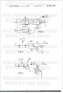 FIG. 3 shows in block diagram form the control circuit SC of FIG. 1.
This control circuit SC comprises a pulse-width modulator stage 10 a first input 11 of which, connected to input 1, receives flyback pulses of positive polarity +VTL from the second secondary winding B3 of the line transformer TL (see FIG. 1 and a second input 12 of which receives a so-called regulating voltage or current whose level is proportional to the difference between the actual output voltage VS and a constant reference value, delivered by the output 32 of a regulating circuit or stage 30 whose input 31 is connected through input 3 to the positive output pole SP of the supply device BS supplying the regulated voltage VS. The variation of the regulating current or voltage causes the variation of the time instant when the instantaneous amplitude of a sawtooth voltage waveform, either with substantially constant slope and amplitude, reaches the level of this regulating voltage, or with a slope variable depending of the regulating current (which is added to the current for linearly charging a capacitor), reaches the predetermined level of a fixed reference (threshold) voltage, with respect to the beginning or the end of the sawtooth waveform. Thus a two-level rectangular signal with constant periodicity is generated, whose duty cycle varies as a function of the regulating current or voltage. If it is arranged, which is possible, for a reduction of the output voltage VS with respect to its nominal value defined by the reference voltage, to cause an increase in the duty cycle and for an increase in VS to have the opposite effect, regulation of this output voltage VS is provided, which tends to be stabilized to this nominal value.
The output 14 of modulator 10 supplies a first input 21 of the driver stage 20 of the first switching transistor T1, a second input 22 of which receives the flyback pulses of negative polarity -VTL, coming from the first secondary winding B2 of the line transformer TL.
FIGS. 4 and 5 illustrate two different embodiments of the driver stage 20 of FIG. 3, providing efficient turn off of the first transistor T1.
In FIG. 4, the driver stage 20A comprises a third supply input 23 which connected to the positive pole (P) of the source of the (unregulated) input voltage VE and to one of the terminals of a first resistor R1 (1.8 kiloohms) whose other terminal is connected in parallel to the anodes of two diodes D2 and D3 (of type 1N4148). The second of these diodes D3 has its cathode connected to the base of a third NPN transistor T2 and to one of the terminals of a second resistor R2 (220 ohms). The emitter of the third transistor T2 is connected to the other terminal of the second resistor R2 and to the output
24 of stage 20A, which is connected through the output 6 of the control
circuit SC to the base of the first transistor T1. The collector of the
second transistor T2 is connected through a third resistor R3 (10 ohms)
to the second input 22 of stage 20A receiving the signal -VTL which
comprises the negative-going flyback pulses and, between them, plateaux
of a constant positive level (zero average value). The base of the first
transistor T1 is coupled to its emitter and to ground G, through a
fourth resistor R4 (100 ohms). The third transistor T2 is thus mounted
as a common collector (emitter-follower) stage.
When the output 14 of modulator 10 (FIG. 3) which is connected to the input 21 of stage 20A supplies a low state (level), i.e. a voltage close to zero, the thus positively biased diode D2 becomes conducting so that its anode will be at a voltage of a few tenths of a volt (0.7+V CEsat ) which is less than the voltage required for making the three series PN junctions orientated in the same direction conductive, the first of which is formed by the third diode D3, the second is the base-emitter junction of a third transistor T2 and the third that of the first transistor T1, which will thus remain turned off. When, on the other hand, output 14 supplies a high state or forms an open circuit (the output stage of modulator 10 being formed by an open-collector transistor), diode D2 is cut off by its reverse bias and the voltage VE applied to the input 23 causes a current to flow through the first resistor R1, the diode D3 and the respective base-emitter junctions of transistors T2 and T1 connected in series. Under these circumstances and if, at the same time, the voltage waveform -VTL applied to the collector of transistor T3 presents its constant positive level portion, coinciding with the trace periods of the horizontal scan, transistors T2 and T1 become simultaneously saturated with the effect previously described insofar as the supply device BS of FIG. 1 is concerned. On the other hand, when the voltage waveform -VTL applied to the collector of the third transistor T2 becomes negative, during flyback periods, the current then flows between terminals 23 and 22 of driver stage 20 A, through resistor R1, diode D3, the base-collector junction of the third transistor T2 and resistor R3. The third transistor T2 then operates along its symmetrical saturation characteristics, i.e. it is inverted so that its collector becomes emitter and vice versa. It then conducts a current in the reverse direction between ground and the input 22 (negative) through the resistor R4 across the terminals of which it causes, after removal of the excess minority carriers from the base of the first transistor T1 through the third transistor T2, a voltage drop biasing said base negatively with respect to the emitter. This negative voltage applied to the base of reversely saturated transistor T3 allows a considerable reduction in the storage time and a rapid turnoff of the first transistor T1. Since the sawtooth generator of the pulse-width
modulator 10 described above is controlled by positive-going flyback
pulses, the rectangular signal applied by its output 14 (FIG. 14) to
input 21 of stage 20A undergoes, during the flyback period following the
turn off of the first transistor T1, a transition from its high state
to its low state which causes diode D2 to conduct and, consequently, the
third transistor T2 (reversed) to be cut off before the waveform -VTL
becomes positive again and rebiases this transistor T2 the right way
round.
FIG. 5 shows the schematic diagram of another embodiment of the driver circuit 20 of FIG. 3, designated by 20B, which has only been modified with respect to circuit 20A of FIG. 4 insofar as the collector circuit of the third transistor T2 and the base circuit of the first transistor T1 are concerned.
This modification is more particularly intented for the case where the negative peak amplitude of the voltage waveform -VTL applied to the base of the first transistor T1 through resistor R3 and the emitter-collector path of the reversely saturated third transistor T2, exceeds the reverse (Zener) avalanche-effect breakdown voltage of one of the base-emitter or base-collector junctions of the first transistor T1. This may occur when the first secondary winding B2 of the line transformer TL is also used for other functions in the television receiver.
To prevent the third transistor T2 from being reversely saturated (symmetrically), the circuit 20B comprises a fourth diode D4 inserted between the input 22 receiving the voltage waveform -VTL and the collector thereof, in series with the resistor R3 and connected to conduct in the same direction as its collector-emitter path. The input 22 is more over connected to the cathode of a fifth diode D5 (1N4148) whose anode is connected through a circuit formed by a fifth resistor R5 (330 ohms) and a third capacitor C3 (1nF) connected in parallel, to the base of the first transistor T1.
Diode D5 isolates the base of transistor T1 from the input 22, when the waveform -VTL is positive, and connects them together through a resistive voltage divider formed by resistors R5 and R4 in series, when it becomes negative. Capacitor C3 accelerates the turn-off by favoring the transmission to the base of T1 of abrupt transitions of the negative flybacd pulses.
 FIG.
6 is a diagram, partly in block form, of a possible embodiment of the
pulse-width modulator 10 of the control circuit SC of FIG. 3. Diagrams
D, E and F of FIG. 7 show the voltage waveforms applied respectively to
the input 11 (+VTL) and supplied by the output SI (VI) of the sawtooth
generator GD and by the output 14 (VP) of circuit 10A.
FIG.
6 is a diagram, partly in block form, of a possible embodiment of the
pulse-width modulator 10 of the control circuit SC of FIG. 3. Diagrams
D, E and F of FIG. 7 show the voltage waveforms applied respectively to
the input 11 (+VTL) and supplied by the output SI (VI) of the sawtooth
generator GD and by the output 14 (VP) of circuit 10A.
Modulator 10A of FIG. 5 comprises a sawtooth generator GD formed by a conventional integrator circuit comprising a first amplifier A1 (integrated operational amplifier, for example), an integrating resistor R1 inserted in series between the input 11 receiving the voltage waveform +VTL illustrated by Diagram D of FIG. 7 and supplied by the second secondary winding B3 of the line transformer TL, and the input (inverting) of amplifier A1, as well as an interating capacitor CI connected between this input and the output SI of amplifier A1 (capacitive feedback). In response to this waveform +VTL, the output of amplifier A1 forming the output SI of sawtooth generator GD, supplies a voltage waveform VI illustrated by the diagram E of FIG. 7 which comprises, during the period between time instants t0 and t2 corresponding to the trace period TA of the scan, a voltage decreasing linearly between a maximum value (positive) and a minimum value (negative), and during the flyback intervals preceding time instant t0 and succeding to time instant t2, an increasing voltage of substantially semi-cosinusoidal shape.
Voltage VI is applied to one of the inputs (-) of an analog voltage comparator which may be formed by means of a second differential-type amplifier A2 (integrated operational amplifier), whose other input (+) connected to the input 12 of modulator 10A, receives the regulating voltage VR supplied by the regulator stage (30 of FIG. 3). This regulating voltage VR, which is obtained by comparing
the output voltage VS of the supply device BS of the circuit of FIG. 1
with a reference voltage (VZ supplied by a Zener diode, for example), is
a DC voltage undergoing slow variations, shown in Diagram E of FIG. 7
by a dash-dot line.
When the waveform VI applied to the inverting input (-) of comparator A2 is greater than the regulating voltage VR, which is the case during the period between time instants t0 and t1, its output connected to the output 14 of modulator 10A provides a low state. When, on the other hand, it (VI) reaches or becomes less than VR, which occurs from the time instant t1, the output 14 of modulator 10A provides a high state (which causes saturation of the first transistor T1). This high state continues until time instant t4 subsequent to the time instant t2 of the beginning of the following flyback pulse whose
leading edge controls the turn-off of the first transistor T1, when the
waveform VI becomes greater than the regulating voltage VR. Thus there
is obtained at the output 14 of modulator 10A a rectangular signal VP
shown in Diagram F of FIG. 7, formed successively of a low-level (zero
or negative) beginning during the first half of the flyback period TR
and ending at time instant t1, and a high level going from time instant
t1 to time instant t4. Time instant t1 of the positive transition of
signal VP, which determines the beginning of conduction of the first
transistor T1 is then situated during the trace period of the scan TA
and its position with respect to the beginning t0 or to the end t2
thereof varies as a function of the regulating voltage VR. When the
regulating voltage VR is negative (as on the Diagram E of FIG. 7), a
predetermined fraction of the output voltage VS is greater than the
reference voltage, the duration of the high level state (t2-t1) is less
than half of the trace period of the scan T1. In the opposite case, this
duration (t2-t1) is greater than TA/2. The modification of this
duration (t2-t1) and thus of the duty cycle is carried out in the
reverse direction of the variation of the output voltage VS so as to
stabilize it at a previously adjusted level, with respect to this
reference voltage. The waveform -VTL may also be applied to the input 11
of modulator 10A. In this case, the input of comparator A2 must also be
inverted.
To obtain suitable operating limits, while taking into consideration particularly the value of inductance L, the duty cycle or the durations (t2-t1) must vary between 0, the case where the input voltage VE is equal to the nominal output voltage VS, and about two-thirds, the case where the maximum power is supplied for a minimum voltage at the input.
The ratio between the residual alternating voltage (hum) at the output and the alternating voltage at the input must also allow an image to be obtained which is not perturbed for the eye. A value less than or equal to a hundredth for this ratio gives satisfactory results.
 FIG.
8 shows the simplified diagram of a practical embodiment (by means of
discrete components) of the pulse-width modulator 10 of FIG. 3.
Different waveforms of a current I1 and input +VTL and output VP
voltages are respectively illustrated by the Diagrams H, J and K of FIG.
9.
FIG.
8 shows the simplified diagram of a practical embodiment (by means of
discrete components) of the pulse-width modulator 10 of FIG. 3.
Different waveforms of a current I1 and input +VTL and output VP
voltages are respectively illustrated by the Diagrams H, J and K of FIG.
9.
The input 11 of modulator 10B of FIG. 3 receives the voltage waveform +VTL which may be suppled either directly by the second secondary winding B3 of line transformer TL, or through a coupling capacitor whose one terminal is connected to the collector of the trace switch transistor TH (see FIG. 1). This input 11 supplies a passive shaping circuit, supplying negative-going (decreasing) sawtooth waveforms during the trace periods of scan T1. This passive circuit comprises a fourth coupling capacitor C4 (0.1μ) one terminal of which is connected to the input 11 and the other of which is connected to one of the terminals of a sixth resistor R6 (10 Kohms). The other terminal of this resistor R6 is connected to one of the terminals of a seventh resistor R7 (5.6 Kohms), to one of the terminals of a fifth capacitor C5 (5.6 nF) and to the anode of a sixth diode D6. The other terminal of capacitor C5 is connected to ground G. The cathode of the sixth diode D6 and the other terminal of resistor R7 are both connected to one of the terminals of an eighth resistor R8 (33 kohms), to that of a ninth resistor R9 (470 ohms), to that of a sixth capacitor C6 (4.7 nF) and to the regulation input 12 of modulator 10B, which is connected to the output 32 of the regulator stage 30 (see FIG. 3). The other terminal of capacitor C6 is connected to ground. The other terminal of resistor R8 is connected to the supply input 13 of modulator 10B receiving the input voltage VE. The other terminal of the ninth resistor R9 is connected to the base of a fourth NPN transistor T3, which forms the voltage comparator stage, whose emitter is connected to ground and whose collector (open), which forms the output 14 of modulator 10 B, is connected to the input 21 of the driver stage 20A (of FIG. 4) or 20B (of FIG. 5), formed by the cathode of the second diode D2. The value of capacitor C6 has been chosen so as to limit the maximum negative voltage applied to the base-emitter junction of transistor T3 to a value less than its reverse avalanche breakdown voltage. When the input voltage waveform+VTL
is positive, as during the major portion of the flyback periods TR,
diode D6 short-circuits resistor R7 and we have then a simple passive RC
integrator formed by resistor R6 in series and two capacitors C5 and C6
in parallel, whose output is connected to the base of transistor T3
through resistor R9. Transistor T3 becomes conducting when its base
current IB formed by the sum of currents I1 and I2 becomes positive. The
current I1 shown by an arrow in FIG. 8 and on the Diagram H of FIG. 9,
results from the application of the +VTL waveform of Diagram J to the
above-mentionned simple integrator, during its positive alternation, and
to the cascaded double integrator R6, C5, R7, C6 during its negative
plateau going from t0 to t2. During this negative voltage plateau of the
+VTL signal, the current I1 becomes negative and linearly decreasing.
When the instantaneous negative amplitude of current I1 becomes equal to
the positive current I2 shown by another arrow in FIG. 8 and by means
of a reversed constant level (-I2) shown by a broken line in diagram H
of FIG. 7, which occurs at time t1, the base current of transistor T3 is
cancelled out and this latter is cut off. Since the current I2 is due
for a large part to the regulating current IR supplied by the output of
the regulator stage (30 in FIG. 3) and proportional to the error
voltage, the duration of the cut-off state (t4-t1) of transistor T3 and,
consequently, that (t2-t1) of the saturated state of the first
transistor T1 (as well as the duty cycle) will vary reversely to the
variation of this current IR. The current IE shown by an arrow in FIG.
8, which flows through the high-value resistor R8 from the input voltage
source VE and which is one of the components with IR of current I2,
forms a small current for maintaining transistor T3 saturated in the
absence of flyback pulses and thus of horizontal deflection. The fact
that resistor R8 is supplied by the unregulated input voltage VE allows
another parameter to be added for acting on the duty cycle of transistor
T3 as a function thereof. Diagram K of FIG. 9 illustrates the
rectangular signal VP obtained at the output 14 of the modulator 10B of
FIG. 8.
 FIG.
10 is a schematic diagram of a conventional regulator stage 30 of the
control circuit of FIG. 3. It is formed essentially by a well-known
circuit called differential amplifier having two inputs, the first of
which receives an adjustable fraction of the voltage to be stabilized,
formed, in the present case, by the output voltage VS of the power
supply device (BS, FIG. 1) and the second input of which receives a
stable reference voltage which is generally generated within this stage
(as in most known ballast or switched-mode voltage regulator).
FIG.
10 is a schematic diagram of a conventional regulator stage 30 of the
control circuit of FIG. 3. It is formed essentially by a well-known
circuit called differential amplifier having two inputs, the first of
which receives an adjustable fraction of the voltage to be stabilized,
formed, in the present case, by the output voltage VS of the power
supply device (BS, FIG. 1) and the second input of which receives a
stable reference voltage which is generally generated within this stage
(as in most known ballast or switched-mode voltage regulator).
The
reference voltage VZ is here produced by means of a Zener diode D7 (of
the BZX83C type having a stabilized Zener voltage of 7.5 V) whose
cathode is connected to the input 31 receiving the output voltage VS of
the device BS (FIG. 1) and whose anode is connected through an eleventh
resistor R11 (10 Kohms) to ground G. The second input of the
differential amplifier used here is formed by the emitter of a fifth PNP
transistor T4 which is connected to the anode of the Zener diode D7.
The voltage (VS-VZ) biasing this emitter is then fixed with respect to
the output voltage VS. The first input of the differential amplifier is
here formed by the base of transistor T4 which is biased by a
voltage-divider circuit, formed from a fifteenth resistor R15 (4.7
Kohms), a potentiometer R16 (5 Kohms) and a fourteenth resistor R14 (22
Kohms) connected in series between the input terminal 31 and ground G.
The base of transistor T4, connected to the slider of potentiometer R16
receives then a previously adjusted fraction of the output voltage VS
supplying the horizontal deflection circuit (SH), so that it forms a
constant current generator supplying a current proportional to its
emitter-base voltage which is equal to the difference (error voltage)
between the reference voltage VZ and the selected fraction of the output
voltage VS supplied by potentiometer R16. The collector of the fourth
transistor T4, connected by a tenth resistor R10 (2.2 Kohms) to the
output 32, supplies then the regulating current IR to the regulating
input (12, FIGS. 3 and 8) of the pulse-width modulator (10 or 10B, FIGS.
3 and 8).
It will be noted here that a feedback circuit comprising a twelfth resistor R12 (5.6 Kohms) and a seventh capacitor C7 (4.7 nF) in series connects the collector of transistor 14 to its base.
The difference between the voltage respectively provided by the potentiometer R16 and the Zener diode D7 causes more or less heavy conduction of transistor T4 which delivers the current IR.
In short, when the output voltage VS increases, the voltage (VS-VZ) at the emitter of transistor T4 increases more than that applied to its base and current IR increases. The value of I1 at which transistor T3 is cut off increases then in absolute value and this transistor T3 is turned off later, which reduces the conducting period of transistor T1. The peak current in inductance L then diminishes, which causes a reduction of the output voltage VS which comes back to its nominal value, taking into account the residual error required for controlled operation.
FIG. 11 shows the complete simplified diagram of a power supply device BS of FIG. 1 whose control circuit SCA is respectively formed by the driver circuit 20A of FIG. 4, by the modulator 10B of FIG. 8 and the regulator stage 30 of FIG. 10, except for a few variations.
The variations concern a damping resistor R17 of 1 kiloohm shunting the inductance L, resistor R8 and resistor R10 which are both connected directly to the base of transistor T3 instead of being connected to the cathode of diode D6, resistor R11 which has been omitted and a resistor R13 which shunts the slider of potentiometer R16 to ground. These details of construction have no influence at all on the operation of the circuit such as it has been described above, but simply allow easier adjustment.
 Another
embodiment is shown in FIG. 12. It allows more especially a television
set to be supplied with power in which the horizontal deflection circuit
operates from a higher DC voltage VS, of about 100 volts for example,
itself obtained from an initial output voltage VSI of about 60 volts.
The operation of the circuit is fundamentally the same as that of FIG.
11 and only the differences will be described below. The components
playing the same role in both diagrams bear the same references. The
values may however be different but their dimensioning is within the
scope of a man skilled in the art. The voltage VS delivered by the power
supply is used principally in the horizontal deflection circuit which
is the component consuming most power in the television set. The power
supply circuit components receiving permanently a voltage when the
horizontal deflection circuit is not operating, but when the mains is
connected, are solely those indispensable for activating the power
supply, i.e. the first switching transistor T1 and the circuit for
measuring the output voltage in the regulator stage 300.
Another
embodiment is shown in FIG. 12. It allows more especially a television
set to be supplied with power in which the horizontal deflection circuit
operates from a higher DC voltage VS, of about 100 volts for example,
itself obtained from an initial output voltage VSI of about 60 volts.
The operation of the circuit is fundamentally the same as that of FIG.
11 and only the differences will be described below. The components
playing the same role in both diagrams bear the same references. The
values may however be different but their dimensioning is within the
scope of a man skilled in the art. The voltage VS delivered by the power
supply is used principally in the horizontal deflection circuit which
is the component consuming most power in the television set. The power
supply circuit components receiving permanently a voltage when the
horizontal deflection circuit is not operating, but when the mains is
connected, are solely those indispensable for activating the power
supply, i.e. the first switching transistor T1 and the circuit for
measuring the output voltage in the regulator stage 300.
To simplify the driver stage 100, instead of the single switching transistor T1, an integrated Darlington circuit T10 is used of the BU 807 type, for example. Therefore, the gain is sufficient to omit a discrete driver transistor T2 and to connect the cathode of diode D3 directly to the base input of T10. The negative -VTH pulses, coming from an intermediate tapping on coil B2 of the line output transformer, are applied directly to the base of T10 through resistor R3 which is connected in series with a diode D9 whose cathode is connected to this intermediate tapping.
Instead of the input voltage VE, the power supply input 4 of the control circuit SCB is fed by a voltage obtained by rectifying the positive half-waves (plateaux) of the -VTL voltage supplied by the first secondary winding B2, by means of a diode D8 and a capacitor C8. Thus considerably lower voltage may be obtained than that supplying the horizontal deflection circuit, of the order of 13 volts, for example. A voltage of this value allows video amplification circuits as well as other circuits
of the television set to be supplied while providing for these latter a
very great reliability. This voltage is applied through resistor R1 to
the anodes of diodes D2 and D3 and through resistor R8 to the base of
the transistor T3 of modulator 10B.
The regulator stage 300 here comprises two PNP transistors T4 and T5 connected differentially. For that, their emitters receive the voltage rectified by D8 through a resistor R18 of 1.5 kiloohms. The collector of transistor T5 is connected to ground through a resistor R20 of 3.9 kiloohms and the collector of transistor T4, which supplies the regulating current IR, is connected to the cathode of diode D6 through a resistor R10 of 4.7 kiloohms.
The reference voltage (6.2 volts) is supplied by a Zener diode D7 whose anode is connected to ground, and cathode to a resistor R19 (6.8 kiloohms) which receives the voltage rectified by D8. This reference voltage is applied to the base of transistor 14. A capacitor C9 (49 microfarads) shunts diode D7 so as to cause the reference voltage to rise gradually when the apparatus is switched on, which allows a gradual rise of the output voltage VS to be obtained.
A potentiometer R16 of 10 kiloohms connected between two stopper resistors R15 (68 kiloohms) and R14 (5.6 kiloohms) receives the voltage VS through the resistor R15 and is connected to ground through resistor R14. The sliding contact of potentiometer R16 allows a fraction of the voltage VS to be applied to the base T5. A resistor R13 (47 kiloohms) also connects this base to the common point between R15 and R16.
An anti-oscillation capacitor C10 (15 nanofarads) connects the base of the collector of transistor T5.
Thus the regulating current IR supplied by resistor R10 is directly dependent on the difference between the output voltage VS, applied to the horizontal deflection circuit, and the reference voltage determined by the Zener diode D7. The power supply BS thus stabilizes this voltage VS and at the same time the rectified voltage supplied by diode D8.
To
stop this power supply, as well as that of FIG. 11 moreover, it is
sufficient to stop by means of a remote control receiver, for example,
the operation of the horizontal oscillator.
In this case, the input voltage VE is still present, but is considerably smaller than voltage VS. For the power supply of FIG. 12, this reduced voltage is only applied to the Darlington transistor T10 and a fraction thereof to the base of transistor T5 of the regulator stage 300. Thus the life expectation of the other components of the device BS is increased. Since the voltage supplied by diode D8 is itself regulated, it may be used for supplying a major portion of the television set, except for the horizontal deflection circuit supplied by voltage VS and the remote control receiver which must be capable of operating permanently (also in the ready state) so as to detect the turn-on control signal. The protection which was mentioned earlier on is then extended to the greatest part of the components of the television set.
It will be noted here that the three stages 10, 20 and 30 of control circuit SC (see FIGS. 1 and 3) may be formed by means of circuits different from those described and shown and which are known per se, and that it is sufficient to have a secondary winding B2 (in addition to the very-high-voltage winding) of the line transformer TL, supplying negative line-flyback pulses which may be used for generating a decreasing or increasing sawtooth voltage waveform as well as for controlling the cutting off of the first switching transistor T1.
 GENERAL BASIC TRANSISTOR LINE OUTPUT STAGE OPERATION:
The basic essentials of a transistor line output stage are shown in Fig. 1(a). They comprise: a line output transformer which provides the d.c. feed to the line output transistor and serves mainly to generate the high -voltage pulse from which the e.h.t. is derived, and also in practice other supplies for various sections of the receiver; the line output transistor and its parallel efficiency diode which form a bidirectional switch; a tuning capacitor which resonates with the line output transformer primary winding and the scan coils to determine the flyback time; and the scan coils, with a series capacitor which provides a d.c. block and also serves to provide slight integration of the deflection current to compensate for the scan distortion that would otherwise be present due to the use of flat screen, wide deflection angle c.r.t.s. This basic circuit is widely used in small -screen portable receivers with little elaboration - some use a pnp output transistor however, with its collector connected to chassis.
Circuit Variations:
Variations to the basic circuit commonly found include: transposition of the scan coils and the correction capacitor; connection of the line output transformer primary winding and its e.h.t. overwinding in series; connection of the deflection components to a tap on the transformer to obtain correct matching of the components and conditions in the stage; use of a boost diode which operates in identical manner to the arrangement used in valve line output stages, thereby increasing the effective supply to the stage; omission of the efficiency diode where the stage is operated from an h.t. line, the collector -base junction of the line output transistor then providing the efficiency diode action without, in doing so, producing scan distortion; addition of inductors to provide linearity and width adjustment; use of a pair of series -connected line output transistors in some large -screen colour chassis; and in colour sets the addition of line convergence circuitry which is normally connected in series between the line scan coils and chassis. These variations on the basic circuit do not alter the basic mode of operation however.
Resonance
The most important fact to appreciate about the circuit is that when the transistor and diode are cut off during the flyback period - when the beam is being rapidly returned from the right-hand side of the screen to the left-hand side the tuning capacitor together with the scan coils and the primary winding of the line output transformer form a parallel resonant circuit: the equivalent circuit is shown in Fig. 1(b). The line output transformer primary winding and the tuning capacitor as drawn in Fig. 1(a) may look like a series tuned circuit, but from the signal point of view the end of the transformer primary winding connected to the power supply is earthy, giving the equivalent arrangement shown in Fig. 1(b).
The Flyback Period:
Since the operation of the circuit depends mainly upon what happens during the line flyback period, the simplest point at which to break into the scanning cycle is at the end of the forward scan, i.e. with the beam deflected to the right-hand side of the screen, see Fig. 2. At
this point the line output transistor is suddenly switched off by the
squarewave drive applied to its base. Prior to this action a linearly
increasing current has been flowing in the line output transformer
primary winding and the scan coils, and as a result magnetic fields have
been built up around these components. When the transistor is switched
off these fields collapse, maintaining a flow of current which rapidly
decays to zero and returns the beam to the centre of the screen. This
flow of current charges the tuning capacitor, and the voltage at A rises
to a high positive value - of the order of 1- 2k V in large -screen
sets, 200V in the case of mains/battery portable sets. The e
beam deflected to the right-hand side of the screen, see Fig. 2. At
this point the line output transistor is suddenly switched off by the
squarewave drive applied to its base. Prior to this action a linearly
increasing current has been flowing in the line output transformer
primary winding and the scan coils, and as a result magnetic fields have
been built up around these components. When the transistor is switched
off these fields collapse, maintaining a flow of current which rapidly
decays to zero and returns the beam to the centre of the screen. This
flow of current charges the tuning capacitor, and the voltage at A rises
to a high positive value - of the order of 1- 2k V in large -screen
sets, 200V in the case of mains/battery portable sets. The e nergy
in the circuit is now stored in the tuning capacitor which next
discharges, reversing the flow of current in the circuit with the result
that the beam is rapidly deflected to the left-hand side of the screen -
see Fig. 3. When the tuning capacitor has discharged, the voltage at A
has fallen to zero and the circuit energy is once more stored in the
form of magnetic fields around the inductive components. One half -cycle
of oscillation has occurred, and the flyback is complete.
nergy
in the circuit is now stored in the tuning capacitor which next
discharges, reversing the flow of current in the circuit with the result
that the beam is rapidly deflected to the left-hand side of the screen -
see Fig. 3. When the tuning capacitor has discharged, the voltage at A
has fallen to zero and the circuit energy is once more stored in the
form of magnetic fields around the inductive components. One half -cycle
of oscillation has occurred, and the flyback is complete.
Energy Recovery:
First Part of Forward Scan The circuit then tries to continue the cycle of oscillation, i.e. the magnetic fields again collapse, maintaining a current flow which this time would charge the tuning capacitor negatively (upper plate). When the voltage at A reaches about -0.6V however the efficiency diode becomes forward biased and switches on. This damps the circuit, preventing further oscillation, but the magnetic fields continue to collapse and in doing so produce a linearly decaying current flow which provides the first part of the forward s can,
the beam returning towards the centre of the screen - see Fig. 4. The
diode shorts out the tuning capacitor but the scan correction capacitor
charges during this period, its right-hand plate becoming positive with
respect to its left-hand plate, i.e. point A. Completion of Forward Scan
When the current falls to zero, the diode will switch off. Shortly
before this state of affairs is reached however the transistor is
switched on. In practice this is usually about a third of the way
through the scan. The squarewave applied to its base drives it rapidly
to saturation, clamping the vol
can,
the beam returning towards the centre of the screen - see Fig. 4. The
diode shorts out the tuning capacitor but the scan correction capacitor
charges during this period, its right-hand plate becoming positive with
respect to its left-hand plate, i.e. point A. Completion of Forward Scan
When the current falls to zero, the diode will switch off. Shortly
before this state of affairs is reached however the transistor is
switched on. In practice this is usually about a third of the way
through the scan. The squarewave applied to its base drives it rapidly
to saturation, clamping the vol tage
at point A at a small positive value - the collector emitter saturation
voltage of the transistor. Current now flows via the transistor and the
primary winding of the line output transformer, the scan correction
capacitor discharges, and the resultant flow of current in the line scan
coils drives the beam to the right-hand side of the screen see Fig. 5.
tage
at point A at a small positive value - the collector emitter saturation
voltage of the transistor. Current now flows via the transistor and the
primary winding of the line output transformer, the scan correction
capacitor discharges, and the resultant flow of current in the line scan
coils drives the beam to the right-hand side of the screen see Fig. 5.
Efficiency:
The transistor is then cut off again, to give the flyback, and the cycle of events recurs. The efficiency of the circuit is high since there is negligible resistance present. Energy is fed into the circuit in the form of the magnetic fields that build up when the output transistor is switched on. This action connects the line output transformer primary winding across the supply, and as a result a linearly increasing current flows through it. Since the width is
dependent on the supply voltage, this must be stabilised.
Harmonic Tuning:
There is another oscillatory action in the circuit during the flyback period. The considerable leakage inductance between the primary and the e.h.t. windings of the line output transformer, and the appreciable self -capacitance present, form a tuned circuit which is shocked into oscillation by the flyback pulse. Unless this oscillation is controlled, it will continue into and modulate the scan. The technique used to overcome this effect is to tune the leakage inductance and the associated capacitance to an odd harmonic of the line flyback oscillation frequency. By doing this the oscillatory actions present at the beginning of the scan cancel. Either third or fifth harmonic tuning is used. Third harmonic tuning also has the effect of increasing the amplitude of the e.h.t. pulse, and is generally used where a half -wave e.h.t. rectifier is employed. Fifth harmonic tuning results in a flat-topped e.h.t. pulse, giving improved e.h.t. regulation, and is generally used where an e.h.t. tripler is employed to produce the e.h.t. The tuning is mainly built into the line output transformer, though an external variable inductance is commonly found in colour chassis so that the tuning can be adjusted. With a following post I will go into the subject of modern TV line timebases in greater detail with other models and technology shown here at Obsolete Technology Tellye !
SABA ULTRACOLOR T56SC44 CHASSIS S110 THOMSON ICC3000 Circuit arrangement for producing a vertical frequency deflection current CLASS D FRAME DEFLECTION CIRCUIT.A
circuit for generating a vertical frequency deflection current for the
electron beams in the picture tube of a television receiver includes a
current sensor resistor having one end connected to direct voltage
potential by two resistors connected in series and a second end
connected to a vertical frequency sawtooth signal by two additional
resistors connected in series. An error signal generator has one input
terminal connected to the junction the first two resistors and another
input terminal connected the junction of the second two resistors. An
output stage supplies the deflection current. The output terminal of
the error signal generator is connected to the input terminal of the
output stage. The error amplifier is a transconductance amplifier
having an output terminal connected to reference potential by a series
connection of a resistor and a capacitor.
1. In a circuit forgenerating
a vertical frequency deflection current for the electron beams in the
picture tube of a television receiver, said circuit including a
current sensor resistor having a first end connected to direct voltage
potential by first and second resistors connected in series at a
first junction and a second end connected to a vertical frequency
sawtooth signal by third and fourth resistors connected in series at a
second junction, an error amplifier having a first input terminal
connected to said first junction and a second input terminal connected
to said second junction, said circuit having an output stage for
supplying said deflection current, an output terminal of said error
amplifier being connected to an input terminal of said output stage,
an improvement wherein:
said error amplifier comprises a transconductance amplifier and wherein said output terminal of said error amplifier is coupled via an RC network formed by a series connection of a resistor and a capacitor to a reference potential.
 2.
The improvement of claim 1 wherein said output stage operates in a
D-operation and further includes a pulse width modulator and an
electronic switch means, the output terminal of said transconductance
amplifier being connected to said RC network.
3. The improvement of claim 1 wherein said output stage
includes an amplifier working in A-B operation and an electronic
switch means, the output terminal of said transconductance amplifier
being connected to said RC network.
4. The improvement of claim 2 wherein the time constant of said RC
network is in an order of magnitude of several lines times of said
picture tube. 5. The improvement
of claim 3 wherein the time constant of the RC network is in an order
of magnitude of several lines times of said picture tube.
2.
The improvement of claim 1 wherein said output stage operates in a
D-operation and further includes a pulse width modulator and an
electronic switch means, the output terminal of said transconductance
amplifier being connected to said RC network.
3. The improvement of claim 1 wherein said output stage
includes an amplifier working in A-B operation and an electronic
switch means, the output terminal of said transconductance amplifier
being connected to said RC network.
4. The improvement of claim 2 wherein the time constant of said RC
network is in an order of magnitude of several lines times of said
picture tube. 5. The improvement
of claim 3 wherein the time constant of the RC network is in an order
of magnitude of several lines times of said picture tube.
The present invention relates to a switching voltage regulator power supply device
combined with the horizontal deflection circuit of a television
receiver which it supplies with DC voltage. It relates, more
particularly, to DC voltage supply devices of the type which boost or
increase the voltage supplied at the output of the device in relation to
the level of a DC voltage applied to its input and which regulate this
level by recurrent switching of this input voltage, this switching being
synchronous with the (horizontal) line frequency of the television
receiver supplied by this device. 
Switched step-up or boost voltage regulator devices of this type are known, particularly from the publications U.S. Pat. Nos. 3,571,697 (or 3,736,496) and they are related to switched mode power supply devices or DC-DC converters of the so-called unisolated flyback type, in which the collector-emitter path of a bipolar switching transistor is connected in series with a commutating inductance between the terminals of a DC source supplying an input voltage and a rectifying diode is connected between the junction of the inductance with the transistor and one of the plates of a filtering or storage capacitor (in parallel with the load), so that the current stored in the inductance during the conducting period of the transistor is used for charging the capacitor (and supplying the load) through the diode during its consecutive cut-off period. The use of a switched-mode power supply device of this type in television receivers for supplying, particularly, the horizontal deflection circuit thereof has been described, for example, in two articles by VAN SCHAIK entitled respectively "AN INTRODUCTION TO SWITCHED-MODE POWER SUPPLIES IN TV RECEIVERS" and "CONTROL CIRCUITS FOR SMPS IN TV RECEIVERS," appearing respectively on pages 93 to 108 of No. 3, Vol. 34, of September 1976 and on pages 162 to 180 of No. 4 of this same volume, of December 1976, in the English language Dutch review "ELECTRONIC APPLICATIONS BULLETIN" of PHILIPS', or on pages 181 to 195 of No. 135 of July 1977 and on pages 210 to 226 of No. 136 of October 1977 of the British review "MULLARD TECHNICAL COMMUNICATIONS." Since none of the switched-mode power supply devices described in these articles, isolated or not from the mains, whether they use a forward or a flyback converter, supplies at its output a DC voltage for supplying the horizontal deflection circuit before the switching transistor has been turned on (saturated or conducting) one or more times, the control circuit of this transistor must comprise an independent relaxation oscillator and must be supplied by the same DC input voltage (rectified and smoothed voltage of the AC mains) as the switching circuit comprising the inductance and the transistor in series. Synchronization of the switching with the horizontal deflection can only occur subsequently, when the horizontal oscillator and/or the horizontal deflection circuit as a whole have begun to operate, as soon as the supply voltage supplied thereto by the device which operates independently on starting up, has become sufficient. This synchronization of the switching with the horizontal deflection, advantageous for reducing or eliminating the interferences visible on the screen which are caused by high-frequency energy radiation due to abrupt transition
s of power switching, particularly
when the switching transistor is being cutt off, is generally carried
out by means of a signal comprising flyback or retrace pulses, taken at
the terminals of an auxiliary secondary winding of the line tranformer
whose primary winding is generally connected between the output of the
switched-mode power supply device and one of the terminals of the trace
switch which is provided in the output stage. It is also possible to use
for this purpose the signal provided by the horizontal oscillator (see,
for example, the publication FR-A-2 040 217). In a switched-mode supply for a television receiver described in the publication FR-A-2 261 670, the circuit for controlling the switching transistor of a forward-type converter, supplied with the rectified and smoothed voltage of the mains, comprises a bistable trigger circuit of flip-flop one of whose outputs is coupled back to one of its trigger inputs through a regulating circuit comprising a sawtooth voltage generator and a voltage comparator providing transitions which control the setting of the flip-flop, when the sawtooth voltage reaches the level of a voltage proportional to the amplitude of the flyback pulse. The other one of the two complementary outputs of this flip-flop is coupled back to its other trigger input through a so-called starting loop comprising an ascending voltage wave-form which approaches asymptotically a predetermined voltage level smaller than a predetermined fraction of the nominal level which the amplitude of the flyback pulse must reach in normal operation, and a voltage comparator providing transitions which control the recurrent resetting of the flip-flop to its initial state until the flyback pulse has reached or exceeded a threshold amplitude slightly below its nominal amplitude. When this threshold amplitude has been exceeded, resetting of the flip-flop is controlled by the flyback pulses themselves, negative-going in the present case, which supplant the starting pulses. Such an arrangement is equivalent to an astable multivibrator during the starting period, which later becomes a monostable one and triggered by the flyback pulses and whose quasi-stable state has a variable duration, depending on the amplitude of these pulses so as to obtain regulation thereof by the duty cycle. The pulse which controls the closing of the switch (saturation of the switching transistor) begins here with the leading edge of the flyback pulse and its duration or length is modulated as a function of the current drawn by the load and of the variation of the rectified and smoothed voltage, so that its end controlling the opening of the supply switch
(cutting off the transistor) occurs during the trace portion of the
horizontal deflection. Thus it can be seen that this switched-mode
supply, like most of the known ones, effects regulation of its output
voltage by varying the duty cycle as a reverse function of the level
thereof. Since the high-frequency radiation is precisely at its most intense during abrupt transitions of current in the switching inductance and of the voltage accross its terminals, the appearance of one or more vertical lines (light or dark according to the sense of the modulation of the carrier wave by the video signal) may be observed, contrasting with the normal contents of the picture, whose location on the screen depends on the duration of the pulse controlling the switching transistor. The effect of this radiation becomes particularly troublesome when the input signal of the radio-frequency stages or tuner is small, particularly when the selected channel is situated in the lower part of the VHF band, for the automatic gain-control device of the re
ceiver acts on the gain of the high-frequency and/or
intermediate-frequency input stages, so that the sensitivity
(amplification) of the receiver is then maximum and this also as
concerns the spurious radiated signals. SUMMARY OF THE INVENTION
The present invention, on the one hand, avoids or at least appreciably reduces the interferences visible on the screen by controlling the cutting off of the switching transistor in synchronism with the leading edge or the flyback pulse and, on the other hand, the starting of the horizontal deflection circuit by means of a simple circuit without any special oscillator, and provides efficient protection of the switching transistor which remains cut off when the horizontal deflection circuit is not operating. This is made possible by using a step-up switching regulator supply device of the type described in the publication U.S. Pat. No. 3,571,697 and whose control circuit includes, in accordance with the invention, the horizontal deflection circuit, which it supplies.
The object of the present invention is a power supply device with boosting and regulation of its output voltage by switching, combined with a horizontal sweep circuit of a television receiver, which it supplies and which comprises a horizontal oscillator, a driver stage and an output stage including a line transformer, this device comprising an inductance and the collector-emitter path of a switching transistor connected in series between the poles of a DC input voltage source, a rectifiying diode connected by its anode to the junction between the inductance and the collector of the transistor and by its cathode to one of the terminals of a filtering capacitor whose other terminal is connected to the emitter of the transistor so as to supply between its terminals an initial output voltage, slightly lower than the input voltage, when the transistor is cut off permanently, and a regulated DC output voltage with a level higher than the input voltage, when the transistor is recurrently alternately turned on and off, the level of this output voltage depending on the duty cycle of the respective states of this transistor, and a control circuit for driving the base of the transistor and including a regulator stage comparing an adjustable fraction of the output voltage to a fixed reference voltage and supplying a regulating current or voltage proportional to the difference between these compared voltages, to a pulse-width modulator triggered by means a recurrent signal and supplying a rectangular signal whose duty cycle varies as a function of this regulating current or voltage, and another driver stage receiving the rectangular signal and controlling the switching transistor.
In accordance with the invention, the horizontal deflection forming an integral part of the circuit controlling the switching transistor, determines therefor, from the start, the repetition period of the rectangular signal controlling it, and one of the supply inputs of the other driver stage receives directly a first voltage waveform whose positive alternations, comprise DC voltage plateaux
and
whose negative alternations comprise negative-going flyback pulses
supplied by a first secondary winding of the line transformer, so as to
control the cut-off the switching transistor substantially
simultaneously with that of the trace switch transistor. DESCRIPTION OF THE DRAWINGS
The invention will be better understood and other of its objects, characteristics, features and advantages will become clear from the following description and the accompanying drawings which refer thereto, given solely by way of example, in which:
FIG. 1 is partly a block diagram and partly a schematic diagram of a power supply device combined with the horizontal deflection circuit in accordance with the invention;
FIG. 2 shows waveforms of two voltages and of a current at different points of the circuit of FIG. 1;
FIG. 3 is a block diagram of the circuit for controlling the switching transistor;
FIGS. 4 and 5 are schematic diagrams of two different embodiments of the driver circuit 20 forming the output stage of the control circuit of FIG. 3;
FIG. 6 is the block diagram of one embodiment of the pulse-width modulator 10 of the circuit of FIG. 3;
FIG. 7 shows three voltage waveforms at different points of the circuit of FIG. 6;
FIG. 8 is a schematic diagram of one embodiment of the pulse-width modulator 10 of the circuit of FIG. 3, using discrete components;
FIG. 9 shows a current waveform and two voltage waveforms at different points of the circuit of FIG. 8;
FIG. 10 is a schematic diagram of a conventional embodiment of a regulator stage 30 adapted to supply the modulation input of the modulator of FIG. 8; and
FIGS. 11 and 12 are partial respective schematic diagrams of two embodiments of a power supply device in accordance with the invention.
DESCRIPTION OF THE PREFERRED EMBODIMENTS
FIG.
1 shows the schematic diagram of the power stages of the power supply
device and of the horizontal deflection circuit of the television
receiver, which it supplies and in block diagram form the respective
circuits which control them. The DC input voltage VE which is not regulated is supplied by a rectifier bridge R with four diodes, supplied at its input by the secondary winding of an insulating step-down transformer TS, whose primary winding is supplied by the AC mains. The output terminals of rectifier bridge R are connected respectively to the terminals of a first filtering capacitor C1 across which this input voltage VE is taken.
The positive pole P of this source of the input voltage VE is connected to one of the terminals of an energy-storage inductance L, whereas its negative pole N is connected to ground G of the receiver, which is isolated from the mains. The other terminal of inductance L is connected, on the one hand, to the collector of a first NPN bipolar switching transistor T1, whose emitter is connected to ground G and, on the other hand, to the anode of a first diode D1 whose cathode is connected to the positive terminal of a second filtering and storage capacitor C2. With the negative terminal of this second capacitor C2 connected to ground G, the output voltage VS which supplies the load is taken between its terminals.
Such a supply device BS provides both step-up or boost and regulation of its output voltage level, because the first switching transistor T1 and the first diode D1 thereof are connected so as to conduct respectively currents flowing through inductance L in the same direction, it supplies at its output formed by the terminals of the second capacitor C2, an initial DC voltage VSI as soon as the primary winding of the insulating transformer TS is connected to the mains. This initial voltage VSI which is equal to the input voltage VE less the forward voltage drop VD1 across the first diode D1, is then supplied to the load until the control circuit SC is started up, whose output 6 is connected to the base of the first transistor T1 so as to cause it to be alternately turned on and off.
When the first transistor T1 is turned on by positively biasing its base-emitter junction, its collector-emitter path connects the junction of the inductance L with the anode of the first diode D1 to ground G. Diode D1 being then reversely biased, it ceases to conduct and the inductance L connected by the first transistor T1 between the positive P and negative N poles of the source supplying the unregulated DC input voltage VE, then conducts a linearly increasing current IL so as to store the energy which increases with the square of the conduction duration of the first transistor T1, until this latter is cut off. At the instant when the first transistor T1 is cut off after the control circuit SC has brought its base-emitter voltage to zero or below, the voltage at the terminals of inductance L is reversed so that, at its junction with the collector of transistor T1 and the anode of diode D1, there appears a voltage VM greater than the input voltage VE, which results in the forward biasing of diode D1. Consequently, from the instant when transistor T1 is cut off, diode D1 conducts a linearly decreasing current until the energy stored in the form of a current IL in the inductance L, which charges the second capacitor C2 to an output voltage VS greater than the input voltage VE, disappears. The regulation of the level of the output voltage VS is here effected in a conventional way, by varying the duty cycle, i.e. the radio (quotient) between the duration of the conducting period of transistor T1 and the sum of the respective durations of two of its successive conducting and cut off periods, as a function of the desired output voltage VS (determined by comparison to a stable reference voltage).
According to the invention, a supply device BS of the above-described type is combined with the horizontal deflection circuit SH of a television receiver, which it supplies, so that this latter forms an integral part of its control circuit SC and for determining the repetition period of its operation and so that the above-mentioned regulation by varying the duty cycle maintains a stable peak-to-peak amplitude of the sawtooth scanning current and/or the very high voltage for biasing the electrodes (anode, focusing electrode and accelerating grid) of the cathode-ray tube, which are obtained by rectifying the horizontal flyback pulses supplied by a step-up secondary winding (not shown) of the line transformer TL.
The horizontal deflection circuit SH which comprises in cascade the horizontal oscillator OH whose known phase control circuit with respect to the horizontal sync signal separated from the composite video signal has not been shown here, the driver stage HD controlled by the horizontal oscillator OH and controlling the output stage OS of the horizontal deflection, is as a whole supplied by the above-described regulated power supply device BS. In fact, the positive supply input AL of the horizontal deflection circuit SH is connected by means of a fuse FS to the junction of the cathode of the first diode D1 with the positive terminal of the second capacitor C2, which forms the positive output terminal SP of the regulated power supply device BS. This supply input AL is connected directly to that of the driver circuit HD and, preferably, through a conventional Zener diode or series ballast transistor voltage regulator VR, to that of the horizontal oscillator OH, which are moreover connected to the isolated ground G.
The supply input AL of the horizontal deflection circuit SH is furthermore connected to one of the primary winding terminals B1 of the line transformer TL, whose other terminal AB is connected in parallel to the collector of another switching transistor TH, of NPN type, called trace switch transistor, to the cathode of a second so-called shun
t
recovery diode DR, to one of the terminals of another capacitor CR,
called line-retrace capacitor, and to one of the plates of an additional
capacitor CS, called trace capacitor, which supplies the horizontal
deflection coils LH one terminal of which is connected to its other
terminal during the trace periods of the scanning. The emitter of the
scanning transistor TH, the anode of the "shunt" recovery diode DR, the
other terminal of the retrace capacitor CR and the other terminal of the
horizontal deflection coils LH are all connected to ground G. This
assembly of components thus connected forms the output stage OS whose
operation is well-known and does not form part of the invention. As was mentioned above, as soon as the primary winding of the step-down isolating transformer TS is connected to the mains, rectifier R supplies the first filtering capacitor C1 so as to provide between its terminals P and N a unregulated low DC voltage VE. With the first transistor T1 then turned off, this input voltage is applied through the inductance L and the first diode D1 to the second capacitor C2 so as to obtain between the terminal SP and ground G an initial output voltage VSI substantially equal to VE-VD1, which is approximately equal to 60 percent of the regulated output voltage VS. This initial output voltage VSI (equal to about 0.6 VS) is sufficient to cause the generation of autonomous oscillations by the horizontal oscillator OH. This latter supplies at its output, connected to the input of driver circuit HD, pulses at an independent frequency close to the line frequency. In response to these pulses, driver circuit HD, also supplied by device BS, provides at the base of the trace switch transistor TH pulses controlling its periodical cut off at this independent frequency and its consecutive turning on after a period greater than the duration of the flyback period, so that the recovery diode DR may take the current from the deflector LH during substantially the first half of the trace portion of the scan. During flyback or retrace, with both transistor TH and diode DR cut off, the energy stored in the form of currents respectively in the inductances of deflector LH and of the primary winding B1 of the line transformer TL which are then, from the AC current point of view, connected in parallel, flow in an oscillating manner through the retrace capacitor CR which forms therewith a parallel resonant circuit whose resonance period determines the duration of the flyback period.
There then appears periodically between point AB and ground G a voltage pulse VTH having substantially a sinusoidal half-wave form, which is shown in Diagram A of FIG. 2. The average value of this voltage VTH being then equal to VSI, at start-up, and to VS, during established operation. The line transformer TL comprises, in addition to a very-high-voltage winding and other windings for supplying rectifying circuits, not shown, two secondary windings B2, B3 respectively supplying across their terminals, voltage waveforms comprising flyback pulses with zero average values and with respectively negative and positive polarities.
This means that the first secondary winding B2 supplies a voltage waveform -VTL which, between two successive flyback pulses, comprises a positive plateau whose level is equal to the average value of these pulses and which is used, in accordance with the invention, to control the turn off of the first transistor T1 so that the interferences which would otherwise be visible only occur during the line-blanking periods comprising the line-retrace periods. The second secondary winding B3 then supplies a voltage waveform +VTL which is the reverse of or complementary to the preceding one -VTL.
One of the terminals of each of these secondary windings B2, B3 is connected to ground G, whereas their other terminals are respectively connected to two inputs 2 and 1 of the control circuit SC. A third input 3 of this latter is connected to the SP output of the supply device BS and a fourth input 4 is connected to the positive pole P of the input voltage source VE. A fifth terminal 5 of the control circuit SC is connected to ground G (or negative pole N) and its output 6 is connected to the base of the first transistor T1. This control circuit SC causes, following the start up of the horizontal deflection circuit SH, a first saturation of the first transistor T1 at a time determined by a pulse-width modulator operating by conventional comparison of a sawtooth voltage waveform the elaboration of which is controlled by a first flyback pulse, with a regulating voltage, depending on the output voltage VS. During this saturation period of transistor T1 which extends as far as the leading edge of the next flyback pulse, energy is stored in inductance L.
From the instant when transistor T1 is turned off, diode D1 transfers this stored energy to the second capacitor C2, at the terminals of which it causes an increase of the voltage VS with respect to its initial value VSI, until the current in diode D1 is canceled out, when it becomes reverse biased.
The collector-emitter voltage waveforms VTH of the trace switch transistor TH and VCE of the switching transistor T1 in established operation have been shown respectively by the diagrams A and B of FIG. 2. Diagram C of FIG. 2 shows the corresponding waveform of the current IL flowing through the inductance L.
When the base of the first transistor T1 receives from the output 6 of the control circuit SC a rectangular signal which turns it on at time instant t1, its collector-emitter voltage VCE (Diagram B) becomes close to zero (V CEsat ) and a linearly increasing current IL (Diagram C) flows through inductance L from time t1 until time t2 when transistor T1 is again turned off, which is controlled by the leading edge of the flyback pulse VTH (Diagram A). With the collector current of transistor T1 canceled at the end of the storage time of the excess minority carriers in the base, the voltage across the terminals of the inductance L inverses its polarity so as to be added to the input voltage VE, so that the collector-emitter voltage VCE (Diagram B) then reaches a level VM greater than VS (as well as VE), so as to apply forward bias to the first diode D1, which then conducts the current IL through the inductance L. This current IL, from time instant t2 when it reaches its maximum value IM, becomes linearly decreasing and it flows through the first diode D1 in the passing direction in order to recharge
the second capacitor C2 and supply, in
particular, the horizontal deflection circuit SH. When the current IL passing through the first diode D1 is canceled out at time t3, the collector-emitter voltage VCE of the first transistor T1 becomes equal to the unregulated input voltage VE until the next turn on of the transistor T1, and the first diode D1 remains reversely biased until the time when this latter is cut off again.
From the above it can be easily seen that the principal advantage of this combined device resides in the fact that a single oscillator OH belonging to the horizontal deflection circuit SH is sufficient for controlling the two power switching transistors TH and T1.
Furthermore, a possible overload in the circuitry of the television receiver, such for example as a short-circuit of the trace switch transistor TH, results in overloading the diode D and the inductance L. The first transistor T1 which is consequently cut off is not subjected to this overload and is therefore protected. In order to protect the rest of the television receiver as well as inductance L and the first diode D1, a fuse FS may be connected in series in the supply line from the second capacitor C2. This fuse FS may also be inserted between pole P and inductance L.
It is moreover known that it is difficult to construct switched supplies for obtaining correct operation when it is not fully charged (for supplying, for example, a ready-state remote-control receiver). In the present case, the problem does not come up since, when the supply is in operation, there is always a minimum load formed by the horizontal deflection circuit. When this circuit is not operating, the supply circuit BS does not operate either, but it supplies an output voltage VSI of a value less than the nominal voltage VS which cannot cause damage and which may, for example, supply a ready-state receiver for television receivers having a remote control.
Finally, the control circuit SC allows transistor T1 to be cut off at the beginning of each flyback period, when the blanking circuit has extinguished the spot (s) on the cathode-ray tube. Thus, the spurious signals radiated into the receiver input circuits will cause no visible effect on the screen of the cathode-ray tube.
 FIG. 3 shows in block diagram form the control circuit SC of FIG. 1.
 This control circuit SC comprises a pulse-width modulator stage 10 a first input 11 of which, connected to input 1, receives flyback pulses of positive polarity +VTL from the second secondary winding B3 of the line transformer TL (see FIG. 1 and a second input 12 of which receives a so-called regulating voltage or current whose level is proportional to the difference between the actual output voltage VS and a constant reference value, delivered by the output 32 of a regulating circuit or stage 30 whose input 31 is connected through input 3 to the positive output pole SP of the supply device BS supplying the regulated voltage VS. The variation of the regulating current or voltage causes the variation of the time instant when the instantaneous amplitude of a sawtooth voltage waveform, either with substantially constant slope and amplitude, reaches the level of this regulating voltage, or with a slope variable depending of the regulating current (which is added to the current for linearly charging a capacitor), reaches the predetermined level of a fixed reference (threshold) voltage, with respect to the beginning or the end of the sawtooth waveform. Thus a two-level rectangular signal with constant periodicity is generated, whose duty cycle varies as a function of the regulating current or voltage. If it is arranged, which is possible, for a reduction of the output voltage VS with respect to its nominal value defined by the reference voltage, to cause an increase in the duty cycle and for an increase in VS to have the opposite effect, regulation of this output voltage VS is provided, which tends to be stabilized to this nominal value.
The output 14 of modulator 10 supplies a first input 21 of the driver stage 20 of the first switching transistor T1, a second input 22 of which receives the flyback pulses of negative polarity -VTL, coming from the first secondary winding B2 of the line transformer TL.
FIGS. 4 and 5 illustrate two different embodiments of the driver stage 20 of FIG. 3, providing efficient turn off of the first transistor T1.
In FIG. 4, the driver stage 20A comprises a third supply input 23 which connected to the positive pole (P) of the source of the (unregulated) input voltage VE and to one of the terminals of a first resistor R1 (1.8 kiloohms) whose other terminal is connected in parallel to the anodes of two diodes D2 and D3 (of type 1N4148). The second of these diodes D3 has its cathode connected to the base of a third NPN transistor T2 and to one of the terminals of a second resistor R2 (220 ohms). The emitter of the third transistor T2 is connected to the other terminal of the second resistor R2 and to the o
utput
24 of stage 20A, which is connected through the output 6 of the control
circuit SC to the base of the first transistor T1. The collector of the
second transistor T2 is connected through a third resistor R3 (10 ohms)
to the second input 22 of stage 20A receiving the signal -VTL which
comprises the negative-going flyback pulses and, between them, plateaux
of a constant positive level (zero average value). The base of the first
transistor T1 is coupled to its emitter and to ground G, through a
fourth resistor R4 (100 ohms). The third transistor T2 is thus mounted
as a common collector (emitter-follower) stage. When the output 14 of modulator 10 (FIG. 3) which is connected to the input 21 of stage 20A supplies a low state (level), i.e. a voltage close to zero, the thus positively biased diode D2 becomes conducting so that its anode will be at a voltage of a few tenths of a volt (0.7+V CEsat ) which is less than the voltage required for making the three series PN junctions orientated in the same direction conductive, the first of which is formed by the third diode D3, the second is the base-emitter junction of a third transistor T2 and the third that of the first transistor T1, which will thus remain turned off. When, on the other hand, output 14 supplies a high state or forms an open circuit (the output stage of modulator 10 being formed by an open-collector transistor), diode D2 is cut off by its reverse bias and the voltage VE applied to the input 23 causes a current to flow through the first resistor R1, the diode D3 and the respective base-emitter junctions of transistors T2 and T1 connected in series. Under these circumstances and if, at the same time, the voltage waveform -VTL applied to the collector of transistor T3 presents its constant positive level portion, coinciding with the trace periods of the horizontal scan, transistors T2 and T1 become simultaneously saturated with the effect previously described insofar as the supply device BS of FIG. 1 is concerned. On the other hand, when the voltage waveform -VTL applied to the collector of the third transistor T2 becomes negative, during flyback periods, the current then flows between terminals 23 and 22 of driver stage 20 A, through resistor R1, diode D3, the base-collector junction of the third transistor T2 and resistor R3. The third transistor T2 then operates along its symmetrical saturation characteristics, i.e. it is inverted so that its collector becomes emitter and vice versa. It then conducts a current in the reverse direction between ground and the input 22 (negative) through the resistor R4 across the terminals of which it causes, after removal of the excess minority carriers from the base of the first transistor T1 through the third transistor T2, a voltage drop biasing said base negatively with respect to the emitter. This negative voltage applied to the base of reversely saturated transistor T3 allows a considerable reduction in the storage time and a rapid turnoff of the first transistor T1. Since the sawtooth generator of the pulse-widt
h
modulator 10 described above is controlled by positive-going flyback
pulses, the rectangular signal applied by its output 14 (FIG. 14) to
input 21 of stage 20A undergoes, during the flyback period following the
turn off of the first transistor T1, a transition from its high state
to its low state which causes diode D2 to conduct and, consequently, the
third transistor T2 (reversed) to be cut off before the waveform -VTL
becomes positive again and rebiases this transistor T2 the right way
round. FIG. 5 shows the schematic diagram of another embodiment of the driver circuit 20 of FIG. 3, designated by 20B, which has only been modified with respect to circuit 20A of FIG. 4 insofar as the collector circuit of the third transistor T2 and the base circuit of the first transistor T1 are concerned.
This modification is more particularly intented for the case where the negative peak amplitude of the voltage waveform -VTL applied to the base of the first transistor T1 through resistor R3 and the emitter-collector path of the reversely saturated third transistor T2, exceeds the reverse (Zener) avalanche-effect breakdown voltage of one of the base-emitter or base-collector junctions of the first transistor T1. This may occur when the first secondary winding B2 of the line transformer TL is also used for other functions in the television receiver.
To prevent the third transistor T2 from being reversely saturated (symmetrically), the circuit 20B comprises a fourth diode D4 inserted between the input 22 receiving the voltage waveform -VTL and the collector thereof, in series with the resistor R3 and connected to conduct in the same direction as its collector-emitter path. The input 22 is more over connected to the cathode of a fifth diode D5 (1N4148) whose anode is connected through a circuit formed by a fifth resistor R5 (330 ohms) and a third capacitor C3 (1nF) connected in parallel, to the base of the first transistor T1.
Diode D5 isolates the base of transistor T1 from the input 22, when the waveform -VTL is positive, and connects them together through a resistive voltage divider formed by resistors R5 and R4 in series, when it becomes negative. Capacitor C3 accelerates the turn-off by favoring the transmission to the base of T1 of abrupt transitions of the negative flybacd pulses.
 FIG.
6 is a diagram, partly in block form, of a possible embodiment of the
pulse-width modulator 10 of the control circuit SC of FIG. 3. Diagrams
D, E and F of FIG. 7 show the voltage waveforms applied respectively to
the input 11 (+VTL) and supplied by the output SI (VI) of the sawtooth
generator GD and by the output 14 (VP) of circuit 10A.
FIG.
6 is a diagram, partly in block form, of a possible embodiment of the
pulse-width modulator 10 of the control circuit SC of FIG. 3. Diagrams
D, E and F of FIG. 7 show the voltage waveforms applied respectively to
the input 11 (+VTL) and supplied by the output SI (VI) of the sawtooth
generator GD and by the output 14 (VP) of circuit 10A. Modulator 10A of FIG. 5 comprises a sawtooth generator GD formed by a conventional integrator circuit comprising a first amplifier A1 (integrated operational amplifier, for example), an integrating resistor R1 inserted in series between the input 11 receiving the voltage waveform +VTL illustrated by Diagram D of FIG. 7 and supplied by the second secondary winding B3 of the line transformer TL, and the input (inverting) of amplifier A1, as well as an interating capacitor CI connected between this input and the output SI of amplifier A1 (capacitive feedback). In response to this waveform +VTL, the output of amplifier A1 forming the output SI of sawtooth generator GD, supplies a voltage waveform VI illustrated by the diagram E of FIG. 7 which comprises, during the period between time instants t0 and t2 corresponding to the trace period TA of the scan, a voltage decreasing linearly between a maximum value (positive) and a minimum value (negative), and during the flyback intervals preceding time instant t0 and succeding to time instant t2, an increasing voltage of substantially semi-cosinusoidal shape.
Voltage VI is applied to one of the inputs (-) of an analog voltage comparator which may be formed by means of a second differential-type amplifier A2 (integrated operational amplifier), whose other input (+) connected to the input 12 of modulator 10A, receives the regulating voltage VR supplied by the regulator stage (30 of FIG. 3). This regulating voltage VR, which is obtained by com
paring
the output voltage VS of the supply device BS of the circuit of FIG. 1
with a reference voltage (VZ supplied by a Zener diode, for example), is
a DC voltage undergoing slow variations, shown in Diagram E of FIG. 7
by a dash-dot line. When the waveform VI applied to the inverting input (-) of comparator A2 is greater than the regulating voltage VR, which is the case during the period between time instants t0 and t1, its output connected to the output 14 of modulator 10A provides a low state. When, on the other hand, it (VI) reaches or becomes less than VR, which occurs from the time instant t1, the output 14 of modulator 10A provides a high state (which causes saturation of the first transistor T1). This high state continues until time instant t4 subsequent to the time instant t2 of the begin
ning of the following flyback pulse whose
leading edge controls the turn-off of the first transistor T1, when the
waveform VI becomes greater than the regulating voltage VR. Thus there
is obtained at the output 14 of modulator 10A a rectangular signal VP
shown in Diagram F of FIG. 7, formed successively of a low-level (zero
or negative) beginning during the first half of the flyback period TR
and ending at time instant t1, and a high level going from time instant
t1 to time instant t4. Time instant t1 of the positive transition of
signal VP, which determines the beginning of conduction of the first
transistor T1 is then situated during the trace period of the scan TA
and its position with respect to the beginning t0 or to the end t2
thereof varies as a function of the regulating voltage VR. When the
regulating voltage VR is negative (as on the Diagram E of FIG. 7), a
predetermined fraction of the output voltage VS is greater than the
reference voltage, the duration of the high level state (t2-t1) is less
than half of the trace period of the scan T1. In the opposite case, this
duration (t2-t1) is greater than TA/2. The modification of this
duration (t2-t1) and thus of the duty cycle is carried out in the
reverse direction of the variation of the output voltage VS so as to
stabilize it at a previously adjusted level, with respect to this
reference voltage. The waveform -VTL may also be applied to the input 11
of modulator 10A. In this case, the input of comparator A2 must also be
inverted. To obtain suitable operating limits, while taking into consideration particularly the value of inductance L, the duty cycle or the durations (t2-t1) must vary between 0, the case where the input voltage VE is equal to the nominal output voltage VS, and about two-thirds, the case where the maximum power is supplied for a minimum voltage at the input.
The ratio between the residual alternating voltage (hum) at the output and the alternating voltage at the input must also allow an image to be obtained which is not perturbed for the eye. A value less than or equal to a hundredth for this ratio gives satisfactory results.
 FIG.
8 shows the simplified diagram of a practical embodiment (by means of
discrete components) of the pulse-width modulator 10 of FIG. 3.
Different waveforms of a current I1 and input +VTL and output VP
voltages are respectively illustrated by the Diagrams H, J and K of FIG.
9.
FIG.
8 shows the simplified diagram of a practical embodiment (by means of
discrete components) of the pulse-width modulator 10 of FIG. 3.
Different waveforms of a current I1 and input +VTL and output VP
voltages are respectively illustrated by the Diagrams H, J and K of FIG.
9. The input 11 of modulator 10B of FIG. 3 receives the voltage waveform +VTL which may be suppled either directly by the second secondary winding B3 of line transformer TL, or through a coupling capacitor whose one terminal is connected to the collector of the trace switch transistor TH (see FIG. 1). This input 11 supplies a passive shaping circuit, supplying negative-going (decreasing) sawtooth waveforms during the trace periods of scan T1. This passive circuit comprises a fourth coupling capacitor C4 (0.1μ) one terminal of which is connected to the input 11 and the other of which is connected to one of the terminals of a sixth resistor R6 (10 Kohms). The other terminal of this resistor R6 is connected to one of the terminals of a seventh resistor R7 (5.6 Kohms), to one of the terminals of a fifth capacitor C5 (5.6 nF) and to the anode of a sixth diode D6. The other terminal of capacitor C5 is connected to ground G. The cathode of the sixth diode D6 and the other terminal of resistor R7 are both connected to one of the terminals of an eighth resistor R8 (33 kohms), to that of a ninth resistor R9 (470 ohms), to that of a sixth capacitor C6 (4.7 nF) and to the regulation input 12 of modulator 10B, which is connected to the output 32 of the regulator stage 30 (see FIG. 3). The other terminal of capacitor C6 is connected to ground. The other terminal of resistor R8 is connected to the supply input 13 of modulator 10B receiving the input voltage VE. The other terminal of the ninth resistor R9 is connected to the base of a fourth NPN transistor T3, which forms the voltage comparator stage, whose emitter is connected to ground and whose collector (open), which forms the output 14 of modulator 10 B, is connected to the input 21 of the driver stage 20A (of FIG. 4) or 20B (of FIG. 5), formed by the cathode of the second diode D2. The value of capacitor C6 has been chosen so as to limit the maximum negative voltage applied to the base-emitter junction of transistor T3 to a value less than its reverse avalanche breakdown voltage. When the input voltage waveform
+VTL
is positive, as during the major portion of the flyback periods TR,
diode D6 short-circuits resistor R7 and we have then a simple passive RC
integrator formed by resistor R6 in series and two capacitors C5 and C6
in parallel, whose output is connected to the base of transistor T3
through resistor R9. Transistor T3 becomes conducting when its base
current IB formed by the sum of currents I1 and I2 becomes positive. The
current I1 shown by an arrow in FIG. 8 and on the Diagram H of FIG. 9,
results from the application of the +VTL waveform of Diagram J to the
above-mentionned simple integrator, during its positive alternation, and
to the cascaded double integrator R6, C5, R7, C6 during its negative
plateau going from t0 to t2. During this negative voltage plateau of the
+VTL signal, the current I1 becomes negative and linearly decreasing.
When the instantaneous negative amplitude of current I1 becomes equal to
the positive current I2 shown by another arrow in FIG. 8 and by means
of a reversed constant level (-I2) shown by a broken line in diagram H
of FIG. 7, which occurs at time t1, the base current of transistor T3 is
cancelled out and this latter is cut off. Since the current I2 is due
for a large part to the regulating current IR supplied by the output of
the regulator stage (30 in FIG. 3) and proportional to the error
voltage, the duration of the cut-off state (t4-t1) of transistor T3 and,
consequently, that (t2-t1) of the saturated state of the first
transistor T1 (as well as the duty cycle) will vary reversely to the
variation of this current IR. The current IE shown by an arrow in FIG.
8, which flows through the high-value resistor R8 from the input voltage
source VE and which is one of the components with IR of current I2,
forms a small current for maintaining transistor T3 saturated in the
absence of flyback pulses and thus of horizontal deflection. The fact
that resistor R8 is supplied by the unregulated input voltage VE allows
another parameter to be added for acting on the duty cycle of transistor
T3 as a function thereof. Diagram K of FIG. 9 illustrates the
rectangular signal VP obtained at the output 14 of the modulator 10B of
FIG. 8.  FIG.
10 is a schematic diagram of a conventional regulator stage 30 of the
control circuit of FIG. 3. It is formed essentially by a well-known
circuit called differential amplifier having two inputs, the first of
which receives an adjustable fraction of the voltage to be stabilized,
formed, in the present case, by the output voltage VS of the power
supply device (BS, FIG. 1) and the second input of which receives a
stable reference voltage which is generally generated within this stage
(as in most known ballast or switched-mode voltage regulator). The
reference voltage VZ is here produced by means of a Zener diode D7 (of
the BZX83C type having a stabilized Zener voltage of 7.5 V) whose
cathode is connected to the input 31 receiving the output voltage VS of
the device BS (FIG. 1) and whose anode is connected through an eleventh
resistor R11 (10 Kohms) to ground G. The second input of the
differential amplifier used here is formed by the emitter of a fifth PNP
transistor T4 which is connected to the anode of the Zener diode D7.
The voltage (VS-VZ) biasing this emitter is then fixed with respect to
the output voltage VS. The first input of the differential amplifier is
here formed by the base of transistor T4 which is biased by a
voltage-divider circuit, formed from a fifteenth resistor R15 (4.7
Kohms), a potentiometer R16 (5 Kohms) and a fourteenth resistor R14 (22
Kohms) connected in series between the input terminal 31 and ground G.
The base of transistor T4, connected to the slider of potentiometer R16
receives then a previously adjusted fraction of the output voltage VS
supplying the horizontal deflection circuit (SH), so that it forms a
constant current generator supplying a current proportional to its
emitter-base voltage which is equal to the difference (error voltage)
between the reference voltage VZ and the selected fraction of the output
voltage VS supplied by potentiometer R16. The collector of the fourth
transistor T4, connected by a tenth resistor R10 (2.2 Kohms) to the
output 32, supplies then the regulating current IR to the regulating
input (12, FIGS. 3 and 8) of the pulse-width modulator (10 or 10B, FIGS.
3 and 8).
FIG.
10 is a schematic diagram of a conventional regulator stage 30 of the
control circuit of FIG. 3. It is formed essentially by a well-known
circuit called differential amplifier having two inputs, the first of
which receives an adjustable fraction of the voltage to be stabilized,
formed, in the present case, by the output voltage VS of the power
supply device (BS, FIG. 1) and the second input of which receives a
stable reference voltage which is generally generated within this stage
(as in most known ballast or switched-mode voltage regulator). The
reference voltage VZ is here produced by means of a Zener diode D7 (of
the BZX83C type having a stabilized Zener voltage of 7.5 V) whose
cathode is connected to the input 31 receiving the output voltage VS of
the device BS (FIG. 1) and whose anode is connected through an eleventh
resistor R11 (10 Kohms) to ground G. The second input of the
differential amplifier used here is formed by the emitter of a fifth PNP
transistor T4 which is connected to the anode of the Zener diode D7.
The voltage (VS-VZ) biasing this emitter is then fixed with respect to
the output voltage VS. The first input of the differential amplifier is
here formed by the base of transistor T4 which is biased by a
voltage-divider circuit, formed from a fifteenth resistor R15 (4.7
Kohms), a potentiometer R16 (5 Kohms) and a fourteenth resistor R14 (22
Kohms) connected in series between the input terminal 31 and ground G.
The base of transistor T4, connected to the slider of potentiometer R16
receives then a previously adjusted fraction of the output voltage VS
supplying the horizontal deflection circuit (SH), so that it forms a
constant current generator supplying a current proportional to its
emitter-base voltage which is equal to the difference (error voltage)
between the reference voltage VZ and the selected fraction of the output
voltage VS supplied by potentiometer R16. The collector of the fourth
transistor T4, connected by a tenth resistor R10 (2.2 Kohms) to the
output 32, supplies then the regulating current IR to the regulating
input (12, FIGS. 3 and 8) of the pulse-width modulator (10 or 10B, FIGS.
3 and 8). It will be noted here that a feedback circuit comprising a twelfth resistor R12 (5.6 Kohms) and a seventh capacitor C7 (4.7 nF) in series connects the collector of transistor 14 to its base.
The difference between the voltage respectively provided by the potentiometer R16 and the Zener diode D7 causes more or less heavy conduction of transistor T4 which delivers the current IR.
In short, when the output voltage VS increases, the voltage (VS-VZ) at the emitter of transistor T4 increases more than that applied to its base and current IR increases. The value of I1 at which transistor T3 is cut off increases then in absolute value and this transistor T3 is turned off later, which reduces the conducting period of transistor T1. The peak current in inductance L then diminishes, which causes a reduction of the output voltage VS which comes back to its nominal value, taking into account the residual error required for controlled operation.
FIG. 11 shows the complete simplified diagram of a power supply device BS of FIG. 1 whose control circuit SCA is respectively formed by the driver circuit 20A of FIG. 4, by the modulator 10B of FIG. 8 and the regulator stage 30 of FIG. 10, except for a few variations.
The variations concern a damping resistor R17 of 1 kiloohm shunting the inductance L, resistor R8 and resistor R10 which are both connected directly to the base of transistor T3 instead of being connected to the cathode of diode D6, resistor R11 which has been omitted and a resistor R13 which shunts the slider of potentiometer R16 to ground. These details of construction have no influence at all on the operation of the circuit such as it has been described above, but simply allow easier adjustment.
 Another
embodiment is shown in FIG. 12. It allows more especially a television
set to be supplied with power in which the horizontal deflection circuit
operates from a higher DC voltage VS, of about 100 volts for example,
itself obtained from an initial output voltage VSI of about 60 volts.
The operation of the circuit is fundamentally the same as that of FIG.
11 and only the differences will be described below. The components
playing the same role in both diagrams bear the same references. The
values may however be different but their dimensioning is within the
scope of a man skilled in the art. The voltage VS delivered by the power
supply is used principally in the horizontal deflection circuit which
is the component consuming most power in the television set. The power
supply circuit components receiving permanently a voltage when the
horizontal deflection circuit is not operating, but when the mains is
connected, are solely those indispensable for activating the power
supply, i.e. the first switching transistor T1 and the circuit for
measuring the output voltage in the regulator stage 300.
Another
embodiment is shown in FIG. 12. It allows more especially a television
set to be supplied with power in which the horizontal deflection circuit
operates from a higher DC voltage VS, of about 100 volts for example,
itself obtained from an initial output voltage VSI of about 60 volts.
The operation of the circuit is fundamentally the same as that of FIG.
11 and only the differences will be described below. The components
playing the same role in both diagrams bear the same references. The
values may however be different but their dimensioning is within the
scope of a man skilled in the art. The voltage VS delivered by the power
supply is used principally in the horizontal deflection circuit which
is the component consuming most power in the television set. The power
supply circuit components receiving permanently a voltage when the
horizontal deflection circuit is not operating, but when the mains is
connected, are solely those indispensable for activating the power
supply, i.e. the first switching transistor T1 and the circuit for
measuring the output voltage in the regulator stage 300. To simplify the driver stage 100, instead of the single switching transistor T1, an integrated Darlington circuit T10 is used of the BU 807 type, for example. Therefore, the gain is sufficient to omit a discrete driver transistor T2 and to connect the cathode of diode D3 directly to the base input of T10. The negative -VTH pulses, coming from an intermediate tapping on coil B2 of the line output transformer, are applied directly to the base of T10 through resistor R3 which is connected in series with a diode D9 whose cathode is connected to this intermediate tapping.
Instead of the input voltage VE, the power supply input 4 of the control circuit SCB is fed by a voltage obtained by rectifying the positive half-waves (plateaux) of the -VTL voltage supplied by the first secondary winding B2, by means of a diode D8 and a capacitor C8. Thus considerably lower voltage may be obtained than that supplying the horizontal deflection circuit, of the order of 13 volts, for example. A voltage of this value allows video amplification circuits as well as other circuit
s
of the television set to be supplied while providing for these latter a
very great reliability. This voltage is applied through resistor R1 to
the anodes of diodes D2 and D3 and through resistor R8 to the base of
the transistor T3 of modulator 10B. The regulator stage 300 here comprises two PNP transistors T4 and T5 connected differentially. For that, their emitters receive the voltage rectified by D8 through a resistor R18 of 1.5 kiloohms. The collector of transistor T5 is connected to ground through a resistor R20 of 3.9 kiloohms and the collector of transistor T4, which supplies the regulating current IR, is connected to the cathode of diode D6 through a resistor R10 of 4.7 kiloohms.
The reference voltage (6.2 volts) is supplied by a Zener diode D7 whose anode is connected to ground, and cathode to a resistor R19 (6.8 kiloohms) which receives the voltage rectified by D8. This reference voltage is applied to the base of transistor 14. A capacitor C9 (49 microfarads) shunts diode D7 so as to cause the reference voltage to rise gradually when the apparatus is switched on, which allows a gradual rise of the output voltage VS to be obtained.
A potentiometer R16 of 10 kiloohms connected between two stopper resistors R15 (68 kiloohms) and R14 (5.6 kiloohms) receives the voltage VS through the resistor R15 and is connected to ground through resistor R14. The sliding contact of potentiometer R16 allows a fraction of the voltage VS to be applied to the base T5. A resistor R13 (47 kiloohms) also connects this base to the common point between R15 and R16.
An anti-oscillation capacitor C10 (15 nanofarads) connects the base of the collector of transistor T5.
Thus the regulating current IR supplied by resistor R10 is directly dependent on the difference between the output voltage VS, applied to the horizontal deflection circuit, and the reference voltage determined by the Zener diode D7. The power supply BS thus stabilizes this voltage VS and at the same time the rectified voltage supplied by diode D8.
To
stop this power supply, as well as that of FIG. 11 moreover, it is
sufficient to stop by means of a remote control receiver, for example,
the operation of the horizontal oscillator. In this case, the input voltage VE is still present, but is considerably smaller than voltage VS. For the power supply of FIG. 12, this reduced voltage is only applied to the Darlington transistor T10 and a fraction thereof to the base of transistor T5 of the regulator stage 300. Thus the life expectation of the other components of the device BS is increased. Since the voltage supplied by diode D8 is itself regulated, it may be used for supplying a major portion of the television set, except for the horizontal deflection circuit supplied by voltage VS and the remote control receiver which must be capable of operating permanently (also in the ready state) so as to detect the turn-on control signal. The protection which was mentioned earlier on is then extended to the greatest part of the components of the television set.
It will be noted here that the three stages 10, 20 and 30 of control circuit SC (see FIGS. 1 and 3) may be formed by means of circuits different from those described and shown and which are known per se, and that it is sufficient to have a secondary winding B2 (in addition to the very-high-voltage winding) of the line transformer TL, supplying negative line-flyback pulses which may be used for generating a decreasing or increasing sawtooth voltage waveform as well as for controlling the cutting off of the first switching transistor T1.
 GENERAL BASIC TRANSISTOR LINE OUTPUT STAGE OPERATION:
The basic essentials of a transistor line output stage are shown in Fig. 1(a). They comprise: a line output transformer which provides the d.c. feed to the line output transistor and serves mainly to generate the high -voltage pulse from which the e.h.t. is derived, and also in practice other supplies for various sections of the receiver; the line output transistor and its parallel efficiency diode which form a bidirectional switch; a tuning capacitor which resonates with the line output transformer primary winding and the scan coils to determine the flyback time; and the scan coils, with a series capacitor which provides a d.c. block and also serves to provide slight integration of the deflection current to compensate for the scan distortion that would otherwise be present due to the use of flat screen, wide deflection angle c.r.t.s. This basic circuit is widely used in small -screen portable receivers with little elaboration - some use a pnp output transistor however, with its collector connected to chassis.
Circuit Variations:
Variations to the basic circuit commonly found include: transposition of the scan coils and the correction capacitor; connection of the line output transformer primary winding and its e.h.t. overwinding in series; connection of the deflection components to a tap on the transformer to obtain correct matching of the components and conditions in the stage; use of a boost diode which operates in identical manner to the arrangement used in valve line output stages, thereby increasing the effective supply to the stage; omission of the efficiency diode where the stage is operated from an h.t. line, the collector -base junction of the line output transistor then providing the efficiency diode action without, in doing so, producing scan distortion; addition of inductors to provide linearity and width adjustment; use of a pair of series -connected line output transistors in some large -screen colour chassis; and in colour sets the addition of line convergence circuitry which is normally connected in series between the line scan coils and chassis. These variations on the basic circuit do not alter the basic mode of operation however.
Resonance
The most important fact to appreciate about the circuit is that when the transistor and diode are cut off during the flyback period - when the beam is being rapidly returned from the right-hand side of the screen to the left-hand side the tuning capacitor together with the scan coils and the primary winding of the line output transformer form a parallel resonant circuit: the equivalent circuit is shown in Fig. 1(b). The line output transformer primary winding and the tuning capacitor as drawn in Fig. 1(a) may look like a series tuned circuit, but from the signal point of view the end of the transformer primary winding connected to the power supply is earthy, giving the equivalent arrangement shown in Fig. 1(b).
The Flyback Period:
Since the operation of the circuit depends mainly upon what happens during the line flyback period, the simplest point at which to break into the scanning cycle is at the end of the forward scan, i.e. with the
 beam deflected to the right-hand side of the screen, see Fig. 2. At
this point the line output transistor is suddenly switched off by the
squarewave drive applied to its base. Prior to this action a linearly
increasing current has been flowing in the line output transformer
primary winding and the scan coils, and as a result magnetic fields have
been built up around these components. When the transistor is switched
off these fields collapse, maintaining a flow of current which rapidly
decays to zero and returns the beam to the centre of the screen. This
flow of current charges the tuning capacitor, and the voltage at A rises
to a high positive value - of the order of 1- 2k V in large -screen
sets, 200V in the case of mains/battery portable sets. The e
beam deflected to the right-hand side of the screen, see Fig. 2. At
this point the line output transistor is suddenly switched off by the
squarewave drive applied to its base. Prior to this action a linearly
increasing current has been flowing in the line output transformer
primary winding and the scan coils, and as a result magnetic fields have
been built up around these components. When the transistor is switched
off these fields collapse, maintaining a flow of current which rapidly
decays to zero and returns the beam to the centre of the screen. This
flow of current charges the tuning capacitor, and the voltage at A rises
to a high positive value - of the order of 1- 2k V in large -screen
sets, 200V in the case of mains/battery portable sets. The e nergy
in the circuit is now stored in the tuning capacitor which next
discharges, reversing the flow of current in the circuit with the result
that the beam is rapidly deflected to the left-hand side of the screen -
see Fig. 3. When the tuning capacitor has discharged, the voltage at A
has fallen to zero and the circuit energy is once more stored in the
form of magnetic fields around the inductive components. One half -cycle
of oscillation has occurred, and the flyback is complete.
nergy
in the circuit is now stored in the tuning capacitor which next
discharges, reversing the flow of current in the circuit with the result
that the beam is rapidly deflected to the left-hand side of the screen -
see Fig. 3. When the tuning capacitor has discharged, the voltage at A
has fallen to zero and the circuit energy is once more stored in the
form of magnetic fields around the inductive components. One half -cycle
of oscillation has occurred, and the flyback is complete.Energy Recovery:
First Part of Forward Scan The circuit then tries to continue the cycle of oscillation, i.e. the magnetic fields again collapse, maintaining a current flow which this time would charge the tuning capacitor negatively (upper plate). When the voltage at A reaches about -0.6V however the efficiency diode becomes forward biased and switches on. This damps the circuit, preventing further oscillation, but the magnetic fields continue to collapse and in doing so produce a linearly decaying current flow which provides the first part of the forward s
 can,
the beam returning towards the centre of the screen - see Fig. 4. The
diode shorts out the tuning capacitor but the scan correction capacitor
charges during this period, its right-hand plate becoming positive with
respect to its left-hand plate, i.e. point A. Completion of Forward Scan
When the current falls to zero, the diode will switch off. Shortly
before this state of affairs is reached however the transistor is
switched on. In practice this is usually about a third of the way
through the scan. The squarewave applied to its base drives it rapidly
to saturation, clamping the vol
can,
the beam returning towards the centre of the screen - see Fig. 4. The
diode shorts out the tuning capacitor but the scan correction capacitor
charges during this period, its right-hand plate becoming positive with
respect to its left-hand plate, i.e. point A. Completion of Forward Scan
When the current falls to zero, the diode will switch off. Shortly
before this state of affairs is reached however the transistor is
switched on. In practice this is usually about a third of the way
through the scan. The squarewave applied to its base drives it rapidly
to saturation, clamping the vol tage
at point A at a small positive value - the collector emitter saturation
voltage of the transistor. Current now flows via the transistor and the
primary winding of the line output transformer, the scan correction
capacitor discharges, and the resultant flow of current in the line scan
coils drives the beam to the right-hand side of the screen see Fig. 5.
tage
at point A at a small positive value - the collector emitter saturation
voltage of the transistor. Current now flows via the transistor and the
primary winding of the line output transformer, the scan correction
capacitor discharges, and the resultant flow of current in the line scan
coils drives the beam to the right-hand side of the screen see Fig. 5.Efficiency:
The transistor is then cut off again, to give the flyback, and the cycle of events recurs. The efficiency of the circuit is high since there is negligible resistance present. Energy is fed into the circuit in the form of the magnetic fields that build up when the output transistor is switched on. This action connects the line output transformer primary winding across the supply, and as a result a linearly increasing current flows through it. Since the width is
dependent on the supply voltage, this must be stabilised.
Harmonic Tuning:
There is another oscillatory action in the circuit during the flyback period. The considerable leakage inductance between the primary and the e.h.t. windings of the line output transformer, and the appreciable self -capacitance present, form a tuned circuit which is shocked into oscillation by the flyback pulse. Unless this oscillation is controlled, it will continue into and modulate the scan. The technique used to overcome this effect is to tune the leakage inductance and the associated capacitance to an odd harmonic of the line flyback oscillation frequency. By doing this the oscillatory actions present at the beginning of the scan cancel. Either third or fifth harmonic tuning is used. Third harmonic tuning also has the effect of increasing the amplitude of the e.h.t. pulse, and is generally used where a half -wave e.h.t. rectifier is employed. Fifth harmonic tuning results in a flat-topped e.h.t. pulse, giving improved e.h.t. regulation, and is generally used where an e.h.t. tripler is employed to produce the e.h.t. The tuning is mainly built into the line output transformer, though an external variable inductance is commonly found in colour chassis so that the tuning can be adjusted. With a following post I will go into the subject of modern TV line timebases in greater detail with other models and technology shown here at Obsolete Technology Tellye !
SABA ULTRACOLOR T56SC
44 CHASSIS S110 THOMSON ICC3000 Circuit arrangement for producing a vertical frequency deflection current CLASS D FRAME DEFLECTION CIRCUIT.A
circuit for generating a vertical frequency deflection current for the
electron beams in the picture tube of a television receiver includes a
current sensor resistor having one end connected to direct voltage
potential by two resistors connected in series and a second end
connected to a vertical frequency sawtooth signal by two additional
resistors connected in series. An error signal generator has one input
terminal connected to the junction the first two resistors and another
input terminal connected the junction of the second two resistors. An
output stage supplies the deflection current. The output terminal of
the error signal generator is connected to the input terminal of the
output stage. The error amplifier is a transconductance amplifier
having an output terminal connected to reference potential by a series
connection of a resistor and a capacitor.1. In a circuit for
generating
a vertical frequency deflection current for the electron beams in the
picture tube of a television receiver, said circuit including a
current sensor resistor having a first end connected to direct voltage
potential by first and second resistors connected in series at a
first junction and a second end connected to a vertical frequency
sawtooth signal by third and fourth resistors connected in series at a
second junction, an error amplifier having a first input terminal
connected to said first junction and a second input terminal connected
to said second junction, said circuit having an output stage for
supplying said deflection current, an output terminal of said error
amplifier being connected to an input terminal of said output stage,
an improvement wherein: 
said error amplifier comprises a transconductance amplifier and wherein said output terminal of said error amplifier is coupled via an RC network formed by a series connection of a resistor and a capacitor to a reference potential.
2.
The improvement of claim 1 wherein said output stage operates in a
D-operation and further includes a pulse width modulator and an
electronic switch means, the output terminal of said transconductance
amplifier being connected to said RC network.
3. The improvement of claim 1 wherein said output stage
includes an amplifier working in A-B operation and an electronic
switch means, the output terminal of said transconductance amplifier
being connected to said RC network.
4. The improvement of claim 2 wherein the time constant of said RC
network is in an order of magnitude of several lines times of said
picture tube. 5. The improvement
of claim 3 wherein the time constant of the RC network is in an order
of magnitude of several lines times of said picture tube.
Description:
This
is a continuation of PCT application PCT/EP 91/00531 filed Mar. 19,
1991 by Rudolf Koblitz and titled "Circuit Arrangement For Producing A
Vertical Frequency Deflection Current".
In modern television receivers, the deflection current is generated by means of a class D amplifier. An electronic switch is triggered by pulse width modulated pulses running at line frequency to periodically switch the deflection coils to frame potential using a line transformer. The deflection current is regulated by an error amplifier, the output terminal of which is connected to one of the input terminals of a pulse width modulator. The other input terminal of the pulse width modulator receives a horizontal frequency sawtooth signal. The error amplifier is connected across one diagonal of a resistance bridge, whereby the two input terminals of the error amplifier are connected to a fixed operating
voltage by equal size resistors. Also, a direct voltage reference
potential and a vertical frequency sawtooth signal, are applied to the
input terminals of the error amplifier by two additional resistors
which are the same size as the other two resistors. A sensing
resistor, having very low resistance, is connected between the two
resistors which are connected to the fixed operating voltage. Such an
arrangement is disadvantageous in that the bridging resistors, the error
amplifier and the DC behavior of the horizontal frequency sawtooth
signal are subject to temperature and other environmental changes. Also,
the various circuit components have inherent tolerances which
frequently negatively impact the stability of the circuit.
It is an object of the invention to eliminate the undesirable effects of such drifting and tolerances so that the stability of the circuit arrangement is reduced to the thermal stability of the resistance bridge and of the input offset behavior of the error amplifier, so that the circuit can be realized by way of integrated circuit technology.
Preferred embodiments are described with reference to the drawings, in which:
FIG. 1 is a first preferred embodiment of the invention.
FIG. 2 is a second preferred embodiment of the invention.
In FIG. 1, a vertical deflection circuit includes vertical deflection coils LV which are connected to an operating direct voltage UB by a current sensor resistor RS which measures the deflection current. The defl ection
coils LV are switched to reference potential by a controllable
electronic switch TH. A winding W of a line transformer ZT and an
inductive impedance L connects the switch to the deflection coils LV.
The junction of the vertical deflection coils LV and the winding W of
the line transformer ZT is connected to frame potential by an
integrated capacitor C2. A diode D is connected in parallel to an
electronic switch TH to permit a reflux, or free-running operation the
circuit. The electronic switch TH is triggered by line frequency pulses
which are pulse width modulated so that the intervals during which
the vertical deflection coils LV are at frame potential, are adapted
to the deflection angle. The line frequency trigger pulses are
supplied by a pulse width modulator PBM having two input terminals.
The negative input terminal is connected to a horizontal frequency
sawtooth signal UH and the positive input terminal is connected to the
signal from an error amplifier FV. The error amplifier-FV has two
input terminals which are wired in a bridge consisting of two pairs of
resistors R1, R1' and R2, R2'. The two resistors R1 and R1' are
connected to the operating voltage UB and a capacitor C1. The current
sensor resistor RS is located between these resistors. One of the two
other branches of the bridge receive a fixed reference potential VDC
from resistor R2 and the other branch receives a vertical frequency
sawtooth signal UV from resistor R2'. The error amplifier FV regulates
the width of the pulses, and thus the deflection current, in such a
way that the bridge voltage Ub is zero.
ection
coils LV are switched to reference potential by a controllable
electronic switch TH. A winding W of a line transformer ZT and an
inductive impedance L connects the switch to the deflection coils LV.
The junction of the vertical deflection coils LV and the winding W of
the line transformer ZT is connected to frame potential by an
integrated capacitor C2. A diode D is connected in parallel to an
electronic switch TH to permit a reflux, or free-running operation the
circuit. The electronic switch TH is triggered by line frequency pulses
which are pulse width modulated so that the intervals during which
the vertical deflection coils LV are at frame potential, are adapted
to the deflection angle. The line frequency trigger pulses are
supplied by a pulse width modulator PBM having two input terminals.
The negative input terminal is connected to a horizontal frequency
sawtooth signal UH and the positive input terminal is connected to the
signal from an error amplifier FV. The error amplifier-FV has two
input terminals which are wired in a bridge consisting of two pairs of
resistors R1, R1' and R2, R2'. The two resistors R1 and R1' are
connected to the operating voltage UB and a capacitor C1. The current
sensor resistor RS is located between these resistors. One of the two
other branches of the bridge receive a fixed reference potential VDC
from resistor R2 and the other branch receives a vertical frequency
sawtooth signal UV from resistor R2'. The error amplifier FV regulates
the width of the pulses, and thus the deflection current, in such a
way that the bridge voltage Ub is zero.
In the FIG. 1 embodiment, a transconductance amplifier, which has the ability to convert an input voltage into an output current, is used as the error amplifier FV. In the example, the transconductance amplifier supplies a
current of 1 to 2 mA per 1 V change in input voltage, i.e. it has a g
of 1 to 2 mA/V. The output terminal of the amplifier FV is connected
to an input stage including an RC network, pulse width generator PBM,
and the switching circuit thyristor TH and diode D. The RC circuit is
composed of a resistor Ra and a capacitor Ca and is connected to the
output terminal of the transconductance amplifier. The RC circuit has a
RC time constant in the order of several line times and therefore
complete correction is carried out in a few lines. In this embodiment
the output stage operates in a D-type operation. In a circuit design
tested in practice, a resistance Ra of 33 kOhm and a capacitance Ca of
15 nF were used. A capacitor Cb is parallel to the RC circuit to
filter out the remaining line frequency components. In this way, the
drift of the horizontal sawtooth signal and the drift of the
electronic switch are eliminated. The resistor Ra of the RC circuit
supplies the P-portion of the PI controller which also guarantees
stability of regulation.
Another prefer red
embodiment is shown in FIG. 2. In this embodiment the output stage is
an amplifier which works in A-B operation. The positive input
terminal of the amplifier V is connected to a fixed reference voltage
Uref. The signal from the transconductance amplifier FV is connected to
the negative, input of terminal of the amplifier V. The same
considerations regarding drift and temperature behavior are valid for
this arrangement as with the preferred embodiment shown in FIG. 1.
red
embodiment is shown in FIG. 2. In this embodiment the output stage is
an amplifier which works in A-B operation. The positive input
terminal of the amplifier V is connected to a fixed reference voltage
Uref. The signal from the transconductance amplifier FV is connected to
the negative, input of terminal of the amplifier V. The same
considerations regarding drift and temperature behavior are valid for
this arrangement as with the preferred embodiment shown in FIG. 1.
COLOR TV SCANNING AND POWER SUPPLY PROCESSOR THOMSON TEA2026
DEFLECTION .CERAMIC 500kHz RESONATOR FREQUENCY
REFERENCE .NO LINE AND FRAME OSCILLATOR ADJUSTMENT
.DUAL PLL FOR LINE DEFLECTION .HIGH PERFORMANCE SYNCHRONIZATION .SUPER SANDCASTLE OUTPUT .VIDEO IDENTIFICATION CIRCUIT .AUTOMATIC 50/60Hz STANDARD IDENTIFICATION
.EXCELLENT INTERLACING CONTROL .SPECIALPATENTED FRAME SYNCHRO DEVICE
FOR VCR OPERATION .FRAME SAW-TOOTH GENERATOR .FRAME PHASE MODULATOR FOR THYRISTOR
SMPS CONTROL .ERROR AMPLIFIER AND PHASE MODULATOR
.SYNCHRONIZATION WITH HORIZONTAL
DEFLECTION .SECURITY CIRCUIT AND START UP PROCESSOR
GENERAL DESCRIPTION
As depicted in Figure 1, the TEA2028 combines 3
major functionsof a TV set as follows :
- Horizontal (line) and vertical (frame) time base
generation for spot deviation. The video signal is
used for the synchronization of both time bases.
- On-chip switching power supply controller synchronized
on line frequency.
This integrated circuit has been implemented in
bipolar I2L technology, and various functions are
digitally processed. In fact, resorting to logic functions
has the advantage of working with pure and
accurate signals while full benefit is drawn from
high integration of logic gates (approx. 110 gates
per mm2).
The main objective is to drive all functions using an
accurate time base generated by a master 500kHz
oscillator.
Also, horizontal and vertical time bases, are obtained
by binary division of reference frequency.
This has the advantage of eliminating the 2 adjustments
which were necessary in former devices.
- MAIN FUNCTIONS
- Detection and extraction of line and frame synchronization
pulses from the composite video
signal.
- Horizontal scanning control and synchronization
by two phase-locked loop devices.
- Video identification.
- 50 or 60Hz standardrecognition for vertical scanning.
- Generation of a self-synchronized frame sawtooth
for 50/60Hz standards.
- Line time constant switching for VCR operation
through an input labeled ”VCR” (Video Cassette
Recorder).
- Control and regulation of a primary-connected
switching power supply by on-chip controller device
combining :
• an error amplifier
• a pulse width modulator synchronized on line
frequency
• a start-up and protection system
- Overall TV set protection input
- Frame blanking and super sandcastle output signals
- Frame blanking safety input for CRT protection in
case of vertical stage failure.
FUNCTIONAL DESCRIPTION
Majority of the on-chip analog functions were computer
simulated and results such as temperature
variation, technological characteristic dispersion
and stability, have led to the enhancement and
implementation of actually employed structures.A
parallel in-depth study of the device implemented
in form of integrated sub-sections is provided to
analyze the overall performance in a TV set.
SABA ULTRACOLOR T56SC44 CHASSIS S110 THOMSON ICC3000 APPLICATION INFORMATION ON FRAME
SCANNING IN SWITCHED MODE:
Fundamentals (see Figure 80)
The secondary winding of EHT transformer provides
the energy required by frame yoke.
The frame current modulation is achieved by
modulating the horizontal saw-tooth current and
subsequent integration by a ”L.C” network to reject
the horizontal frequency component.

General Description
The basic circuit is the phase comparator ”C1”
which compares the horizontal saw-tooth and the
output voltage of Error Amplifier ”A”.
The comparator output will go ”high” when the
horizontal saw-tooth voltage is higher than the ”A”
output voltage. Thus, the Pin 4 output signal is
switched in synchronization with the horizontal frequency
and the duty cycle is modulated at frame
frequency.
A driver stage delivers the current required by the
external power switch.
The external thyristor provides for energy transfer
between transformer and frame yoke.
The thyristor will conduct during the last portion of
horizontal trace phase and for half of the horizontal
retrace.
The inverse parallel-connected diode ”D” conducts
during the second portion of horizontal retrace and
at the beginning of horizontal trace phase.
Main advantages of this system are :
- Power thyristor soft ”turn-on”
Once the thyristor has been triggered, the current
gradually rises from 0 to IP, where IP will reach
the maximumvalue at the end of horizontal trace.
The slope current is determined by, the current
available through the secondary winding, the
yoke impedance and the ”L.C.” filter characteristics.
- Power thyristor soft ”turn-off”
The secondary output current begins decreasing
and falls to 0 at the middle of retrace. The thyristor
is thus automatically ”turned-off”.
- Excellent efficiency of power stage dueto very
low ”turn-on” and ”turn-off” switching losses.
Frame Flyback
During flyback, due to the loop time constant, the
frame yoke current cannot be locked onto the
reference saw-tooth. Thus the output of amplifier
”A” will remain high and the thyristor is blocked.
The scanning current will begin flowing through
diode ”D”. As a consequence, the capacitor ”C”
starts charging upto the flyback voltage.The thyristor
is triggeredas soon as the yoke current reaches
the maximum positive value.
SABA ULTRACOLOR T56SC44 CHASSIS S110 THOMSON ICC3000 / THOMSON TEA2026 Scanning control circuit for a television receiver, with gradual startup
THOMSON TDA4950 TV EAST/WEST CORRECTION CIRCUIT:
DESCRIPTION
The TDA4950 is a monolithic integrated circuit in a
8 pin minidip plastic package designed for use in
the east-west pin-cushion correction by driving a
diode modulator in TV and monitor applications.
LOW DISSIPATION
.SQUARE GENERATOR FOR PARABOLIC
CURRENT
.EXTERNAL KEYSTONE ADJUSTMENT (sym-
metry of the parabola)
.INPUT FOR DYNAMIC FIELD CORRECTION
(beam current change)
.STATIC PICTURE WIDTH ADJUSTMENT
.PULSE-WIDTH MODULATOR
.FINAL STAGE D-CLASS WITH ENERGY RE-
DELIVERY
.PARASITIC
PARABOLA
SUPPRESSION,
DURING FLYBACK TIME OF THE VERTICAL SAWTOOTH.
SABA ULTRACOLOR T56SC44 CHASSIS S110 THOMSON ICC3000 E/W TDA4950 CIRCUIT OPERATION:
A differential amplifier OP1 is driven by a vertical
frequency sawtooth current of ± 33µA which is
produced via an external resistor from the sawtooth
voltage. The non-inverting input of this amplifier is
connected with a reference voltage corresponding
to the DC level of the sawtooth voltage. This DC
voltage should be adjustable for the keystone cor-
rection. The rectified output current of this amplifier
drives the parabola network which provides a para-
bolic output current. This output current produces
the corresponding voltage due to the voltage drop
across the external resistor at pin 7.
If the input is overmodulated (> 40µA) the internal
current is limited to 40µA. This limitation can be
used for suppressing the parasitic parabolic current
generated during the flyback time of the frame
sawtooth.
A comparator OP2 is driven by the parabolic cur-
rent. The second input of the comparator is con-
nected with a horizontal frequency sawtooth
voltage the DC level of which can be changed by
the external circuitry for the adjustment of the pic-
ture width.
The horizontal frequency pulse-width modulated
output signal drives the final stage. It consists of a
class D push-pull output amplifier that drives, via
an external inductor, the diode modulator.
1. A single case having first, second side walls and first, second end walls for housing the circuitry of a radio or television receiver comprising a tuner section wherein the tuner section comprises a VHF section and a UHF section which are disposed about in parallel between said first and second side walls and between an antenna input filter section and a phase locked loop section, data inputs mounted on said first side wall of the case near the phase locked loop section, the VHF section being located next to the first side wall of the case with the data inputs; the phase locked loop section being connected to the tuner section and separated from the tuner section by a first subdivision metal shielding plate;
the antenna input filter section located between an antenna input end on the first end wall of the case and the tuner section;
a second subdividing metal shielding plate for separating the tuner section from the antenna input filter section;
a third subdividing metal shielding plate attached to the first and second subdividing metal shielding plates for providing a separation between the UHF section and the VHF section;
an intermediate frequency amplifier connected to the tuner section and located between the phase locked loop section and the second end wall of the case and separated from the phase locked loop section by a fourth subdividing metal shielding plate, the first, second, third and fourth subdividing shielding plates each comprising
brackets at the top for attaching a cover plate; and,
a demodulator connected to the intermediate frequency amplifier.
2. The single case for housing the circuits of a radio or a television receiver according to claim 1 wherein the phase locked loop section co mprises a quartz oscillator reference source;
a phase detector connected to the reference source;
a low pass filter connected to the output of the phase detector and to the tuner section;
a programmable predivider having its output connected to the phase detector and having an input connected to the tuner section;
a shift register having an output connected to the tuner and having an output connected to the programmable predivider,
wherein the phase locked loop section is disposed near the middle of the case where data inputs are disposed on the case next to the phase locked loop section.
3. The single case for housing the circuits of a radio or a television receiver according to claim 2 wherein the tuner section comprises an oscillator;
a preamplifier; and
a mixer stage connected to the preamplifier and to the oscillator and having its output connected to the intermeidate frequency amplifier; and
a band switch having inputs connected to the shift register and having outputs connected to the preamplifier and to the oscillator.
4. The single case for housing the circuits of a radio or a television receiver according to claim 1 wherein the case comprises metal as a structural element.
5. The single case for housing the circuits of a radio or a television receiver according to claim 1 wherein the case comprises plastic as a structural element.
6. The single case for housing the circuits of a radio or a television receiver according to claim 1 wherein leads between the circuits of the phase locked loop section and a tuner circuit section are at most 5 centimeters.
7. The single case for housing the circuits of a radio or a television receiver according to claim 1 wherein the leads between the circuits of the phase locked loop section and the tuner circuit section are at most 2 centimeters.
1. Field of the Invention
The present invention relates to a receiver stage for a radio or a television receiver comprising a tuner, an intermediate frequency amplifier, a demodulator and a phase locked loop circuit.
2. Brief Description of the Background of the Invention Including Prior Art
Such receivers are provided with a tuner for selecting the different emitter frequencies of the radio and television station signals. These antenna signals fed to the tuner are transformed in the tuner by mixing with an oscillator frequency to an intermediate frequency. The intermediate
frequency signals taken from the tuner are amplified in a following
intermediate frequency amplifier. A demodulator following to the
intermediate frequency amplifier demodulates the high frequency
modulated signal to an audio frequency sound signal or respectively to a
video frequency picture signal, which is fed to the final stages for
reproduction in a loudspeaker or respectively on the screen of a
television set. The individual electronic components such as tuner,
intermediate frequency amplifier and demodulator have been
conventionally disposed in separate component parts and were connected
to each other via lines. These lines have to be shielded and are
expensive for this reason. The required plug connections are susceptible
to disturbances and form the sources of interferences, which can pass
from the outside into the receiver station. Therefore, it has been
taught to gather these named device units in a case. Thus there results
an optimal shielding and the elimination of long connecting lines
subject to the influence of disturbances (German Patent Laid Out DE-AS
No. 1,958,993).
Receiver stations of more recent technology comprise capacitor diodes in the tuning circuits. The tuning voltage required for tuning is generated in this case with the aid of a phase locked loop circuit. This phase locked loop circuit provides a D.C. voltage, which results depending on a preselectable divider ratio of a frequency divider of the phase locked loop circuit. The phase locked loop circuit serving tuning purposes is disposed in a separate device component part. This arrangement with separation from the tuner unit however again results in the disadvantage, that interfering pulses can pass to the lines for the data input of the phase locked loop circuit as well as to the tuning voltage carrying line to the tuner unit, which can interfere with the tuning.
SUMMARY OF THE INVENTION
1. Purposes of the Invention
It is an object of the present invention to eliminate a possibility of disturbances from radio or television receiver apparatus.
It is another object of the present invention to provide a compact device comprising major elements employed in tuning of a radio or television receiver.
It is a further object of the invention to simplify the assembly and servicing of radio and television sets.
These and other objects and advantages of the present invention will become evident from the description which follows.
2. Brief Description of the Invention
The present invention provides a receiver stage for a radio or a television receiver wherein a single case encloses a device which comprises a tuner, an intermediate frequency amplifier connected to the tuner, a demodulator connected to the intermediate frequency amplifier, and a phase locked loop provision connected to the tuner.
The phase locked loop can comprise a reference source, a phase detector connected to the reference source, a low pass filter connected to the output of the phase detector and to the tuner, and a programmable divider having its output connected to the phase detector and having an input connected to the tuner. The phase locked loop can comprise a shift register having an output connected to the programmable predivider. The tuner can comprise an oscillator, a preamplifier and a mixer stage connected to the preamplifier and to the oscillator and having its output connected to the intermediate frequency amplifier. The tuner can comprise a band switch having inputs connected to the shift register and having outputs connected to the preamplifier and to the oscillator.
The case can be comprised of metal and/or plastic as a structural element. The connecting leads between the phase locked amplifier and the tuner can be not more than 5 centimeters and are preferably less than 2 centimeters.
A shielding metal plate can be disposed between the tuner section and the phase locked loop provision area and between the phase locked loop provision area and the intermediate frequency amplifier and
automatic gain control area. In addition, a separating shielding metal
plate can be disposed between an antenna input filter section and the
tuner. Furthermore, a metal shielding plate can be disposed between an
UHF area and a VHF area of the tuner, where this plate is attached to
the plate separating the antenna input filter section from the tuner and
to the metal plate separating the tuner and the phase locked loop
provision area.
The novel features which are considered as characteristic for the invention are set forth in particular in the appended claims. The invention itself, however, both as to its construction and its method of operation, together with additional objects and advantages thereof, will be best understood from the following description of specific embodiments when read in connection with the accompanying drawing.
BRIEF DESCRIPTION OF THE DRAWING
In the accompanying drawing in which is shown one of the various possible embodiments of the present invention:
FIG. 1 is a view of a schematic diagram showing the construction according to the invention,
FIG. 2 is a perspective view of the construction according to the invention .
Corresponding numerals in the Figs. designate corresponding items and features.
DESCRIPTION OF INVENTION AND PREFERRED EMBODIMENTS
 In
accordance with the present invention there is provided a receiver
stage for radio and television receivers with a tuner and an
intermediate frequency amplifier, with a demodulator following to the
intermediate frequency amplifier as well as a phase locked loop circuit
for tuning of tuning circuits provided with capacitance diodes. The
receiver circuits, intermediate frequency stages and the demodulator are
disposed in a case jointly forming a device, which is characterized in
that the phase locked loop circuit is disposed in this case.
In
accordance with the present invention there is provided a receiver
stage for radio and television receivers with a tuner and an
intermediate frequency amplifier, with a demodulator following to the
intermediate frequency amplifier as well as a phase locked loop circuit
for tuning of tuning circuits provided with capacitance diodes. The
receiver circuits, intermediate frequency stages and the demodulator are
disposed in a case jointly forming a device, which is characterized in
that the phase locked loop circuit is disposed in this case.
The signals received by the antenna 1 are amplified in a conventional way in a preamplifier 2. The preamplifier is disposed in the tuner area 26 of the receiver. The output of the preamplifier 2 together with the frequency obtained from an oscillator is mixed to an intermediate frequency in the mixing stage 3. The oscillations are amplified in the intermediate amplifier 5 and are demodulated with the aid of the demodulator 6 and the output signal FBAS of the demodulator 6 can be picked up at the connection 7. The components intermediate amplifier 5 and demodulator 6 form part of an intermediate amplifier and automatic gain control section 24. The recited stages are provided in a case and in a single shielding container possibly of the kind described in the German Patent Laid Out DE-AS No. 1,958,993.
In accordance with the teaching of the invention the device components for the phase locked loop (PLL) circuit 22 including programmable predivider 8, reference source 9, phase detector stage 10 and low pass filter 1 are integrated in the same case 12 for generating the tuning voltage. The reference source can be provided by a voltage controlled or by a current controlled oscillator. The output of the input unit 13 is connected to a shift register 14. The shift register 14 is connected to the band switch 15 and to the predivider 8. The data determined for the selected channel can be entered via an input unit 13 connected from the outside to the case 12. These data can set the predivider 8 as well as the
bandswitch 15. After the input of the data via the data line 16 as well
as via the clock input C1 and the enable input EN these can be
disconnected such that also disturbing pulses cannot any longer
influence the phase locked loop circuit. The elementary devices employed
in the circuits of the present invention are preferably provided by
large scale integrated circuits or very large scale integrated circuits.
The case for the composite device can be constructed in a similar way
as the case taught in German Patent Laid Out DE-AS No. 1,958,993. The
leads between the phase locked loop and the tuning circuit can be quite
small, that is less than about 5 centimeters and preferably less than
about 2 centimeters.
 FIG. 2 shows in more detail and in
perspective the disposition of the individual components. The tune area
26, the phase locked loop provision area 22 and the intermediate
amplifier and automatic gain control section 24 are disposed about
sequentially in a single case having respective subdivided areas 26, 22
and 24. The antenna input 1 enters a section containing an antenna input
filter as a first subdivided area. The signal is fed to a respective
subdivided tuning section for the UHF area 30 and for the VHF area 28.
These areas 28 and 38 are disposed more or less in parallel running from
the antenna input filter section. The areas 28 and 30 are followed by a
phase locked loop area 22, which contains a phase locked loop
integrated circuit 23, a predivider 8 and a quartz oscillator 34. Data
inputs 16 are connected from the outside of the box case 12 to the phase
locked loop provision area 22. An output of the phase locked loop
provision area 22 is fed to the adjoining intermediate amplifier and
automatic gain control section 24. The disposition of the antenna input
filter area 32, followed by parallel tuner sections 28,30, followed in
turn by a phase looked loop area 22 and again followed by and
intermediate amplifier and automatic gain control section 24 provides an
advantageous arrangement, which does not require the production of
separate enclosed components and allows the use of a single case. This
construction is space saving as a handling area would otherwise be
required for the casing of each component. The inventor provides that
the various areas are separated by subdividing electromagnetic shields
36. The subdividing electromagnetic shields 36 can be provided with
brackets 38 for attaching a cover plate of for being mounted in the
case.
FIG. 2 shows in more detail and in
perspective the disposition of the individual components. The tune area
26, the phase locked loop provision area 22 and the intermediate
amplifier and automatic gain control section 24 are disposed about
sequentially in a single case having respective subdivided areas 26, 22
and 24. The antenna input 1 enters a section containing an antenna input
filter as a first subdivided area. The signal is fed to a respective
subdivided tuning section for the UHF area 30 and for the VHF area 28.
These areas 28 and 38 are disposed more or less in parallel running from
the antenna input filter section. The areas 28 and 30 are followed by a
phase locked loop area 22, which contains a phase locked loop
integrated circuit 23, a predivider 8 and a quartz oscillator 34. Data
inputs 16 are connected from the outside of the box case 12 to the phase
locked loop provision area 22. An output of the phase locked loop
provision area 22 is fed to the adjoining intermediate amplifier and
automatic gain control section 24. The disposition of the antenna input
filter area 32, followed by parallel tuner sections 28,30, followed in
turn by a phase looked loop area 22 and again followed by and
intermediate amplifier and automatic gain control section 24 provides an
advantageous arrangement, which does not require the production of
separate enclosed components and allows the use of a single case. This
construction is space saving as a handling area would otherwise be
required for the casing of each component. The inventor provides that
the various areas are separated by subdividing electromagnetic shields
36. The subdividing electromagnetic shields 36 can be provided with
brackets 38 for attaching a cover plate of for being mounted in the
case.
The invention provides advantages by way of the
construction layout. By the elimination of a separate PLLunit, the tuner
receiver part can form a compact unit from the antenna input to the
demodulator output including the electronic components required for the
tuning and the band switching.
It will be understood that each of the elements described above, or two or more together, may also find a useful application in other types of receiver station system configurations and received signal processing procedures differing from the types described above.
While the invention has been illustrated and described as embodied in the context of a receiver for a radio or a television receiver, it is not intended to be limited to the details shown, since various modifications and structural changes may be made without departing in any way from the spirit of the present invention.
Without further analysis, the foregoing will so fully reveal the gist of the present invention that others can, by applying current knowledge, readily adapt it for various applications without omitting features that, from the standpoint of prior art, fairly constitute essential characteristics of the generic or specific aspects of this invention. COMPATIBILITY LIST OF MODELS:
BANG & OLUFSEN BEOVISION M 20
BANG & OLUFSEN BEOVISION MX 2000
BEKO 16228 NX
BRANDT ELECTRONIQUE 22 817 TC
BRANDT ELECTRONIQUE 63 369 T
HITACHI CPT 2282
HITACHI CPT 2284
HITACHI CPT 2684
HITACHI CPT 2685
HITACHI CPT 2688
NORDMENDE COLOR 1532
NORDMENDE COLOR 1537
NORDMENDE COLOR 3437
NORDMENDE COLOR 3437 VT
NORDMENDE COLOR 3437-3 D
NORDMENDE COLOR 3457
NORDMENDE COLOR 3532
NORDMENDE COLOR 3532 VT
NORDMENDE COLOR 3537
NORDMENDE COLOR 3537 PSN
NORDMENDE COLOR 3537 VT
NORDMENDE COLOR 3547
NORDMENDE COLOR 4430
NORDMENDE COLOR 4432
NORDMENDE COLOR 4437
NORDMENDE COLOR 5430 STEREO
NORDMENDE COLOR 5432 STEREO
NORDMENDE COLOR 5437 STEREO
NORDMENDE COLOR 5437-3 D STEREO
NORDMENDE COLOR 5457 STEREO
NORDMENDE COLOR 5472
NORDMENDE COLOR 5477
NORDMENDE COLOR 5532 STEREO
NORDMENDE COLOR 5537 STEREO
NORDMENDE COLOR 5537 VT STEREO
NORDMENDE COLOR 5547 STEREO
NORDMENDE COLOR 5557 STEREO
NORDMENDE COLOR 5572
NORDMENDE COLOR 5577
NORDMENDE COLOR 5577 PSN
NORDMENDE COLOR 5632 STEREO
NORDMENDE COLOR B-6417
NORDMENDE COLOR BISONIC 2436
NORDMENDE COLOR SC 1437
NORDMENDE COLOR STEREO 5038
NORDMENDE COLOR STEREO 5627
NORDMENDE COLOR STEREO 5637
NORDMENDE COLOR STEREO 5647
NORDMENDE COLOR STEREO 5742
NORDMENDE COLOR STEREO 5747
NORDMENDE COLOR STEREO 5757
NORDMENDE COLOR STEREOSONIC 2436
NORDMENDE COLOR TPX 2436
NORDMENDE F 11
NORDMENDE F 11 B
NORDMENDE SPECTRA 4070
NORDMENDE SPECTRA 4072
NORDMENDE SPECTRA 4077
NORDMENDE SPECTRA 5002 STEREO
NORDMENDE SPECTRA 5072
NORDMENDE SPECTRA 5077
NORDMENDE SPECTRA 5172
NORDMENDE SPECTRA 5177
NORDMENDE SPECTRA 8007 STEREO
NORDMENDE SPECTRA 8077
NORDMENDE SPECTRA 8102 STEREO
NORDMENDE SPECTRA 8172
NORDMENDE SPECTRA 8177
NORDMENDE SPECTRA 8327 STEREO
NORDMENDE SPECTRA 8330 STEREO
NORDMENDE SPECTRA 8332 STEREO
NORDMENDE SPECTRA 8337 STEREO
NORDMENDE SPECTRA 8337-3 D
NORDMENDE SPECTRA 8337-3 D STEREO
NORDMENDE SPECTRA 8342 STEREO
NORDMENDE SPECTRA 8347 STEREO
NORDMENDE SPECTRA 8360
NORDMENDE SPECTRA 8362
NORDMENDE SPECTRA 8367
NORDMENDE SPECTRA 8370
NORDMENDE SPECTRA 8372
NORDMENDE SPECTRA 8377
NORDMENDE SPECTRA 8427 STEREO
NORDMENDE SPECTRA 8432 STEREO
NORDMENDE SPECTRA 8437 STEREO
NORDMENDE SPECTRA 8467-PSN
NORDMENDE SPECTRA 8472
NORDMENDE SPECTRA 8477
NORDMENDE SPECTRA 9007 STEREO
NORDMENDE SPECTRA 9432 STEREO
NORDMENDE SPECTRA 9437 STEREO
NORDMENDE SPECTRA 9537 STEREO
NORDMENDE SPECTRA STEREO 4000
NORDMENDE SPECTRA STEREO 4002
NORDMENDE SPECTRA STEREO 4007
NORDMENDE SPECTRA STEREO 5002
NORDMENDE SPECTRA STEREO 5007
NORDMENDE SPECTRA STEREO 5102
NORDMENDE SPECTRA STEREO 5107
NORDMENDE SPECTRA STEREO 5202
NORDMENDE SPECTRA STEREO 5207
NORDMENDE SPECTRA STEREO 8007
NORDMENDE SPECTRA STEREO 8107
NORDMENDE SPECTRA STEREO 8108
NORDMENDE SPECTRA STEREO 8108 VT
NORDMENDE SPECTRA STEREO 9007
NORDMENDE SPECTRA STEREO 9108
SABA ABDY STEREO TC
SABA BREGENZ
SABA CTV6728 S
SABA ELECTRONIC
SABA EXPERT
SABA FREIBURG
SABA FREIBURG STEREO
SABA HIFI SONORAMA TC
SABA HIFI STEREO TC
SABA KONSTANZ STEREO
SABA M 67 S 73
SABA M 67 S 75
SABA P 37 S 27
SABA P 8414 S
SABA SONORAMA TC
SABA STEREO
SABA STEREO BADEN-BADEN
SABA STEREO KONSTANZ
SABA STEREO TC
SABA STEREO TC BADEN-BADEN
SABA STEREO TC KONSTANZ
SABA STEREO TC TRIBERG
SABA STEREO TCITA
SABA T 27 S 81 ST TC
SABA T 51 S 83
SABA T 56 S 25
SABA T 56 S 26
SABA T 56 S 82
SABA T 56 SC 44
SABA T 67 S 25
SABA T 67 S 26
SABA T 67 S 30
SABA T 67 S 32
SABA T 67 S 54 VT
SABA T 67 S 82
SABA T 67 S 83
SABA T 67 S 85
SABA T 67 S 94
SABA T 67 S 95
SABA T 67 SC 44
SABA T 6720 S
SABA T 71 SC 83
SABA T 7566 ST
SABA T 7676 S
SABA T 9677 SC
SABA T 9678 S
SABA TELECOMMANDER
SABA TELECOMMANDER ST
SABA VIDEOTEXT STEREO TC
THOMSON TF 5606 MPG
THOMSON TF 5606 PG
THOMSON TF 6758 PG
THOMSON TF 6758 WPG
In modern television receivers, the deflection current is generated by means of a class D amplifier. An electronic switch is triggered by pulse width modulated pulses running at line frequency to periodically switch the deflection coils to frame potential using a line transformer. The deflection current is regulated by an error amplifier, the output terminal of which is connected to one of the input terminals of a pulse width modulator. The other input terminal of the pulse width modulator receives a horizontal frequency sawtooth signal. The error amplifier is connected across one diagonal of a resistance bridge, whereby the two input terminals of the error amplifier are connected to a fixed operat
ing
voltage by equal size resistors. Also, a direct voltage reference
potential and a vertical frequency sawtooth signal, are applied to the
input terminals of the error amplifier by two additional resistors
which are the same size as the other two resistors. A sensing
resistor, having very low resistance, is connected between the two
resistors which are connected to the fixed operating voltage. Such an
arrangement is disadvantageous in that the bridging resistors, the error
amplifier and the DC behavior of the horizontal frequency sawtooth
signal are subject to temperature and other environmental changes. Also,
the various circuit components have inherent tolerances which
frequently negatively impact the stability of the circuit. It is an object of the invention to eliminate the undesirable effects of such drifting and tolerances so that the stability of the circuit arrangement is reduced to the thermal stability of the resistance bridge and of the input offset behavior of the error amplifier, so that the circuit can be realized by way of integrated circuit technology.
Preferred embodiments are described with reference to the drawings, in which:
FIG. 1 is a first preferred embodiment of the invention.
FIG. 2 is a second preferred embodiment of the invention.
In FIG. 1, a vertical deflection circuit includes vertical deflection coils LV which are connected to an operating direct voltage UB by a current sensor resistor RS which measures the deflection current. The defl
 ection
coils LV are switched to reference potential by a controllable
electronic switch TH. A winding W of a line transformer ZT and an
inductive impedance L connects the switch to the deflection coils LV.
The junction of the vertical deflection coils LV and the winding W of
the line transformer ZT is connected to frame potential by an
integrated capacitor C2. A diode D is connected in parallel to an
electronic switch TH to permit a reflux, or free-running operation the
circuit. The electronic switch TH is triggered by line frequency pulses
which are pulse width modulated so that the intervals during which
the vertical deflection coils LV are at frame potential, are adapted
to the deflection angle. The line frequency trigger pulses are
supplied by a pulse width modulator PBM having two input terminals.
The negative input terminal is connected to a horizontal frequency
sawtooth signal UH and the positive input terminal is connected to the
signal from an error amplifier FV. The error amplifier-FV has two
input terminals which are wired in a bridge consisting of two pairs of
resistors R1, R1' and R2, R2'. The two resistors R1 and R1' are
connected to the operating voltage UB and a capacitor C1. The current
sensor resistor RS is located between these resistors. One of the two
other branches of the bridge receive a fixed reference potential VDC
from resistor R2 and the other branch receives a vertical frequency
sawtooth signal UV from resistor R2'. The error amplifier FV regulates
the width of the pulses, and thus the deflection current, in such a
way that the bridge voltage Ub is zero.
ection
coils LV are switched to reference potential by a controllable
electronic switch TH. A winding W of a line transformer ZT and an
inductive impedance L connects the switch to the deflection coils LV.
The junction of the vertical deflection coils LV and the winding W of
the line transformer ZT is connected to frame potential by an
integrated capacitor C2. A diode D is connected in parallel to an
electronic switch TH to permit a reflux, or free-running operation the
circuit. The electronic switch TH is triggered by line frequency pulses
which are pulse width modulated so that the intervals during which
the vertical deflection coils LV are at frame potential, are adapted
to the deflection angle. The line frequency trigger pulses are
supplied by a pulse width modulator PBM having two input terminals.
The negative input terminal is connected to a horizontal frequency
sawtooth signal UH and the positive input terminal is connected to the
signal from an error amplifier FV. The error amplifier-FV has two
input terminals which are wired in a bridge consisting of two pairs of
resistors R1, R1' and R2, R2'. The two resistors R1 and R1' are
connected to the operating voltage UB and a capacitor C1. The current
sensor resistor RS is located between these resistors. One of the two
other branches of the bridge receive a fixed reference potential VDC
from resistor R2 and the other branch receives a vertical frequency
sawtooth signal UV from resistor R2'. The error amplifier FV regulates
the width of the pulses, and thus the deflection current, in such a
way that the bridge voltage Ub is zero. In the FIG. 1 embodiment, a transconductance amplifier, which has the ability to convert an input voltage into an output current, is used as the error amplifier FV. In the example
, the transconductance amplifier supplies a
current of 1 to 2 mA per 1 V change in input voltage, i.e. it has a g
of 1 to 2 mA/V. The output terminal of the amplifier FV is connected
to an input stage including an RC network, pulse width generator PBM,
and the switching circuit thyristor TH and diode D. The RC circuit is
composed of a resistor Ra and a capacitor Ca and is connected to the
output terminal of the transconductance amplifier. The RC circuit has a
RC time constant in the order of several line times and therefore
complete correction is carried out in a few lines. In this embodiment
the output stage operates in a D-type operation. In a circuit design
tested in practice, a resistance Ra of 33 kOhm and a capacitance Ca of
15 nF were used. A capacitor Cb is parallel to the RC circuit to
filter out the remaining line frequency components. In this way, the
drift of the horizontal sawtooth signal and the drift of the
electronic switch are eliminated. The resistor Ra of the RC circuit
supplies the P-portion of the PI controller which also guarantees
stability of regulation. Another prefer
 red
embodiment is shown in FIG. 2. In this embodiment the output stage is
an amplifier which works in A-B operation. The positive input
terminal of the amplifier V is connected to a fixed reference voltage
Uref. The signal from the transconductance amplifier FV is connected to
the negative, input of terminal of the amplifier V. The same
considerations regarding drift and temperature behavior are valid for
this arrangement as with the preferred embodiment shown in FIG. 1.
red
embodiment is shown in FIG. 2. In this embodiment the output stage is
an amplifier which works in A-B operation. The positive input
terminal of the amplifier V is connected to a fixed reference voltage
Uref. The signal from the transconductance amplifier FV is connected to
the negative, input of terminal of the amplifier V. The same
considerations regarding drift and temperature behavior are valid for
this arrangement as with the preferred embodiment shown in FIG. 1.COLOR TV SCANNING AND POWER SUPPLY PROCESSOR THOMSON TEA2026
DEFLECTION .C
ERAMIC 500kHz RESONATOR FREQUENCY
REFERENCE .NO LINE AND FRAME OSCILLATOR ADJUSTMENT
.DUAL PLL FOR LINE DEFLECTION .HIGH PERFORMANCE SYNCHRONIZATION .SUPER SANDCASTLE OUTPUT .VIDEO IDENTIFICATION CIRCUIT .AUTOMATIC 50/60Hz STANDARD IDENTIFICATION
.EXCELLENT INTERLACING CONTROL .SPECIALPATENTED FRAME SYNCHRO DEVICE
FOR VCR OPERATION .FRAME SAW-TOOTH GENERATOR .FRAME PHASE MODULATOR FOR THYRISTOR
SMPS CONTROL .ERROR AMPLIFIER AND PHASE MODULATOR
.SYNCHRONIZATION WITH HORIZONTAL
DEFLECTION .SECURITY CIRCUIT AND START UP PROCESSOR
GENERAL DESCRIPTION
As depicted in Figure 1, the TEA2028 combines 3
major functionsof a TV set as follows :
- Horizontal (line) and vertical (frame) time base
generation for spot deviation. The video signal is
used for the synchronization of both time bases.
- On-chip switching power supply controller synchronized
on line frequency.
This integrated circuit has been implemented in
bipolar I2L technology, and various functions are
digitally processed. In fact, resorting to logic functions
has the advantage of working with pure and
accurate signals while full benefit is drawn from
high integration of logic gates (approx. 110 gates
per mm2).
The main objective is to drive all functions using an
accurate time base generated by a master 500kHz
oscillator.
Also, horizontal and vertical time bases, are obtained
by binary division of reference frequency.
This has the advantage of eliminating the 2 adjustments
which were necessary in former devices.
- MAIN FUNCTIONS
- Detection and extraction of line and frame synchronization
pulses from the com
posite videosignal.
- Horizontal scanning control and synchronization
by two phase-locked loop devices.
- Video identification.
- 50 or 60Hz standardrecognition for vertical scanning.
- Generation of a self-synchronized frame sawtooth
for 50/60Hz standards.
- Line time constant switching for VCR operation
through an input labeled ”VCR” (Video Cassette
Recorder).
- Control and regulation of a primary-connected
switching power supply by on-chip controller device
combining :
• an error amplifier
• a pulse width modulator synchronized on line
frequency
• a start-up and protection system
- Overall TV set protection input
- Frame blanking and super sandcastle output signals
- Frame blanking safety input for CRT protection in
case of vertical stage failure.
FUNCTIONAL DESCRIPTION
Majority of the on-chip analog functions were computer
simulated and results such as temperature
variation, technological characteristic dispersion
and stability, have led to the enhancement and
implementation of actually employed structures.A
parallel in-depth study of the device implemented
in form of integrated sub-sections is provided to
analyze the overall performance in a TV set.
SABA ULTRACOLOR T56SC44 CHASSIS S110 THOMSON ICC3000 APPLICATION INFORMATION ON FRAME
SCANNING IN SWITCHED MODE:
Fundamentals (s
ee Figure 80)The secondary winding of EHT transformer provides
the energy required by frame yoke.
The frame current modulation is achieved by
modulating the horizontal saw-tooth current and
subsequent integration by a ”L.C” network to reject
the horizontal frequency component.

General Description
The basic circuit is the phase comparator ”C1”
which compares the horizontal saw-tooth and the
output voltage of Error Amplifier ”A”.
The comparator output will go ”high” when the
horizontal saw-tooth voltage is higher than the ”A”
output voltage. Thus, the Pin 4 output signal is
switched in synchronization with the horizontal frequency
and the duty cycle is modulated at frame
frequency.
A driver stage delivers the current required by the
external power switch.
The external thyristor provides for energy transfer
between transformer and frame yoke.
The thyristor will conduct during the last portion of
horizontal trace phase and for half of the horizontal
retrace.
The inverse parallel-connected diode ”D” conducts
during the second portion of horizontal retrace and
at the beginning of horizontal trace phase.
Main advantages of this system are :
- Power thyristor soft ”turn-on”
Once the thyristor has been triggered, the current
gradually rises from 0 to IP, where IP will reach
the maximumvalue at the end of horizontal trace.
The slope current is determined by, the current
available through the secondary winding, the
yoke impedance and the ”L.C.” filter characteristics.
- Power thyristor soft ”turn-off”
The secondary output current begins decreasing
and falls to 0 at the middle of retrace. The thyristor
is thus automatically ”turned-off”.
- Excellent efficiency of power stage dueto very
low ”turn-on” and ”turn-off” switching losses.
Frame Flyback
During flyback, due to the loop time constant, the
frame yoke current cannot be locked onto the
reference saw-tooth. Thus the output of amplifier
”A” will remain high and the thyristor is blocked.
The scanning current will begin flowing through
diode ”D”. As a consequence, the capacitor ”C”
starts charging upto the flyback voltage.The thyristor
is triggeredas soon as the yoke current reaches
the maximum positive value.
SABA ULTRACOLOR T56SC44 CHASSIS S110 THOMSON ICC3000 / THOMSON TEA2026 Scanning control circuit for a television receiver, with gradual startup
This invention concerns television scanning circuits.
It involves a scanning startup circuit comprising a capacitor, and means of gradual charging or discharging, to produce a priority voltage transmitted at startup to replace a control voltage, regulating a chopped power supply circuit which is to be started up progressively. At the end of a certain period of time, the regulation control voltage takes over from the original voltage which, at startup, is at a level such that it prevents over-consumption of current in power components. The circuit is also protected against voltage surges, being halted and restarted automatically and gradually in the event of such a surge.
1. In a television receiver comprising a switched mode power supply and a scanning control circuit, said power supply circuit comprising a power switching element (T2) and a pulse-width modulator (24, 26) having an input for receiving a modulating voltage and an output for providing pulses of modulated width, wherein said scanning control circuit comprises, in view of ensuring gradual start-up of scanning:
supply terminals for receiving a low voltage supply (Vcc),
a capacitor (C3) having a first plate and a second plate which are connected to said supply terminals in such a way that upon starting up of the receiver, said first plate will follow the rising potential of one supply terminal,
a voltage limiter (38) to limit the voltage on said capacitor first plate to a predetermined value Vz,
an analogic voltage transmission device (32) having a first input connected to said capacitor first plate, a second input for receiving a control voltage which may vary between predetermined limits, and an output which is connected to the input of said pulse width modulator, said voltage transmission device being designed so that its output will transmit either the voltage on its first input or the voltage on its second input, depending on the relative magnitude of
these voltages, the transmitted voltage being the one which
corresponds to the narrower pulse width at the output of the pulse
width modulator,
the value of Vz being such that it corresponds to a pulse width narrower than the minimum pulse width that may be produced by the modulator when said modulator receives the said control voltage from the transmission device,
means (34) for progressively altering the electrical charge of said capacitor so as to vary the potential of its first plate in a sense corresponding to an increase of the pulse width defined by this voltage.
2. A
circuit as claimed in claim 1 wherein said second plate of the
capacitor is directly connected to said one supply terminal.
3. A circuit as claimed in claim 1,
wherein said means for progressively altering the charge of said
capacitor comprises a current source controlled so as to supply
current to the capacitor only when receiving fly-back pulses
indicating that horizontal scanning is operating.
4. A circuit as claimed in claim 1 further comprising
a threshold comparator (62) having one input receiving said low
voltage supply and another input connected to a voltage reference, and
an output for supplying to the pulse width modulator a disabling
signal whenever said low voltage supply falls below a predetermined
value (VS2). 5. A circuit as
claimed in claim 3, wherein a second means for gradually altering the
electrical charge of said capacitor is provided, said second means
comprising a current source connected to the capacitor in such a way
that it will change the voltage on the first plate in a sense
corresponding to a decrease of the pulse width defined by this
voltage.
television scanning circuits.It involves a scanning startup circuit comprising a capacitor, and means of gradual charging or discharging, to produce a priority voltage transmitted at startup to replace a control voltage, regulating a chopped power supply circuit which is to be started up progressively. At the end of a certain period of time, the regulation control voltage takes over from the original voltage which, at startup, is at a level such that it prevents over-consumption of current in power components. The circuit is also protected against voltage surges, being halted and restarted automatically and gradually in the event of such a surge.
1. In a television receiver comprising a switched mode power supply and a scanning control circuit, said power supply circuit comprising a power switching element (T2) and a pulse-width modulator (24, 26) having an input for receiving a modulating voltage and an output for providing pulses of modulated width, wherein said scanning control circuit comprises, in view of ensuring gradual start-up of scanning:
supply terminals for receiving a low voltage supply (Vcc),
a capacitor (C3) having a first plate and a second plate which are connected to said supply terminals in such a way that upon starting up of the receiver, said first plate will follow the rising potential of one supply terminal,
a voltage limiter (38) to limit the voltage on said capacitor first plate to a predetermined value Vz,
an analogic voltage transmission device (32) having a first input connected to said capacitor first plate, a second input for receiving a control voltage which may vary between predetermined limits, and an output which is connected to the input of said pulse width modulator, said voltage transmission device being designed so that its output will transmit either the voltage on its first input or the voltage on its second input, depending on the relative magnitude o
f
these voltages, the transmitted voltage being the one which
corresponds to the narrower pulse width at the output of the pulse
width modulator, the value of Vz being such that it corresponds to a pulse width narrower than the minimum pulse width that may be produced by the modulator when said modulator receives the said control voltage from the transmission device,
means (34) for progressively altering the electrical charge of said capacitor so as to vary the potential of its first plate in a sense corresponding to an increase of the pulse width defined by this voltage.
2. A
circuit as claimed in claim 1 wherein said second plate of the
capacitor is directly connected to said one supply terminal.
3. A circuit as claimed in claim 1,
wherein said means for progressively altering the charge of said
capacitor comprises a current source controlled so as to supply
current to the capacitor only when receiving fly-back pulses
indicating that horizontal scanning is operating.
4. A circuit as claimed in claim 1 further comprising
a threshold comparator (62) having one input receiving said low
voltage supply and another input connected to a voltage reference, and
an output for supplying to the pulse width modulator a disabling
signal whenever said low voltage supply falls below a predetermined
value (VS2). 5. A circuit as
claimed in claim 3, wherein a second means for gradually altering the
electrical charge of said capacitor is provided, said second means
comprising a current source connected to the capacitor in such a way
that it will change the voltage on the first plate in a sense
corresponding to a decrease of the pulse width defined by this
voltage.
Description:
This
invention concerns television receivers, and more specifically
circuits to control the sweep of the light spot produced on the
television screen. In particular, it relates to the way in which such
circuits start up when the receiver is switched on.
A television receiver usually contains a horizontal scan transformer, surrounded by several closely interconnected circuits:
stabilized supply circuit, providing a regulated DC voltage of about 100 volts, to supply the transformer;
horizontal scan control circuit supplying periodical signals to the base of a transistor mounted in series with the primary transformer winding, with a horizontal deflection coil connected to this transistor;
vertical deflection control circuit using a secondary winding of the horizontal scan transformer as source of supply, to produce a periodical voltage gradient for vertical scanning;
very high voltage circuit using a secondary winding of the transformer to create a high potential in the cathode-ray tube, for the purpose of producing and accelerating the electron beam.
In one embodiment, described in French patent application No. 81 08 337 of Apr. 27, 1981 on the present applicant's behalf, these different circuits are closely interconnected and precise provision has to be made for their startup and stoppage, taking account of their reciprocal interactions.
 FIG.
1 shows the general layout of the horizontal and vertical scanning
circuit, with a regulated chopped power supply circuit. This invention
applies specifically to such a circuit. Further details are to be
found in the aforementioned patent application, but the general
structure will be described here, in order to define the purposes of
this invention.
FIG.
1 shows the general layout of the horizontal and vertical scanning
circuit, with a regulated chopped power supply circuit. This invention
applies specifically to such a circuit. Further details are to be
found in the aforementioned patent application, but the general
structure will be described here, in order to define the purposes of
this invention.
The horizontal scan transformer TL is provided with a primary winding EP, connected on one side to the collector of a transistor T1, the emitter of which is earthed, and on the other side to the output of a stabilized chopped power supply circuit, which is itself powered by the AC mains current.
A horizontal scanning control circuit 10 supplies the base of transistor T1 with periodical signals, synchronized with a synchronization signal SL, extracted by a synchronization extractor (not shown here) from the video signal reaching the receiver.
The transistor collector T1 is connected to a horizontal deflection coil 12, which produces a periodical deflection of the electronic beam of the tube at every changeover of transistor T1.
Transformer TL contains one or more secondary windings, e.g. one winding to produce a very high voltage THT, and another to activate a vertical deflection circuit. A line return signal RL, a negative pulse produced whenever the beam returns as a result of sudden blocking of transistor T1, is taken from one of these windings. This negative pulse RL is used for the horizontal scanning circuit 10, since scanning is synchronized with the syncronization signal SL by shifting the transistor T1 control signals until SL and RL are synchronized. The same pulse RL is also used to operate the chopped power supply circuit.
The vertical deflection circuit 14 is connected to a vertical deflection coil 16, and to a secondary winding of the transformer TL, and is also connected to the horizontal scanning control circuit, to ensure the necessary correspondence between line scanning and frame scanning.
The chopped power supply ciruit, comprises, following a transformer 18 powered by the mains, a rectifier bridge 20 followed by a filter capacitor C1 and inductance L1, mounted in series with the collector of a
transistor T2, the emitter of which is connected to earth.
The collector of this transistor T2 is connected to the anode of a diode 22, the cathode of which is connected to a capacitor C2. The supply circuit output voltage reaches the terminals of this capacitor C2. The supply circuit functions by means of high-frequency switching (at the horizontal scan frequency) of transistor T2, by means of periodical signals (line scanning period 64 microseconds).
Capacitor C2 forms an energy accumulator, which discharges into the utilization circuit while transistor T2 is conducting, and which recharges through inductance L1 when transistor T2 is blocked; the width of the signals is automatically regulated, so that the charge lost every time transistor T2 becomes conducting is exactly counterbalanced by the charge regained during each blocking.
Regulation is obtained by taking a regulation control voltage at the supply circuit output, and comparing it with a stabilized reference voltage, the difference between them being amplified in a differential amplifier 30, and compared in a comparator 24 with a periodical sweep voltage, DSC, supplied at the line scan frequency by a generator 26, which to this effect receives signals at this frequency from the horizontal scanning circuit 10.
The comparator thereby supplies variable-width signals at this frequency, and these are amplified in an amplifier 28, and delivered to the base of transistor T2.
Finally, since transistor T2 has to block a high current every period, the strongly negative line return pulse RL from the secondary winding of
transformer TL is delivered to its base. As already stated, RL is
synchronized with the horizontal scanning signals from circuit 10, and
therefore with returns of the sweep voltage DSC, so that a negative
pulse encouraging blocking of transistor T2 appears immediately after
delivery of a blocking signal from comparator 24.
The electronic control circuits are supplied with low-voltage DC current Vcc, obtainable either by rectifying a fraction of the mains AC current, or by taking a fraction of the DC voltage from the stabilized chopped power supply circuit, or even by a combination of both methods.
In conclusion, close interconnections exist among the chopped power supply circuit (operating at the horizontal scanning frequency), horizontal scanning circuit, vertical scanning circuit, and even very-high-voltage circuits. This invention is intended to perform the following functions relevant to this situation.
First, it is preferable for vertical scanning to function whenever horizontal scanning is in operation (something that involves the appearance of a very high voltage); otherwise, a motionless bright horizontal line is created on the screen, and this will ultimately burn out the photosensitive layer of the television tube.
Second, on startup of the chopped power supply circuit, when the receiver is first switched on, the regulation system will tend to make the comparator 24 generate signals of maximum length, until the supply circuit has reached its nominal output voltage. Current in transistor T2 increases in a linear way (because of inductance L1) during the period of the signal, resulting in far too high a consumption of current in the transistor during supply circuit startup, and serious overheating of the transistor, which has to cut out this high current (several amps) at high voltage (several hundred volts). In any case, the duration of these signals needs to be limited, for normal functioning of the supply circuit (e.g. by ensuring that the regulation control voltage cannot fall below a certain threshold). However, such limitation, although adequate during normal operation, does not eliminate the risk of destruction of transistor T2 during startup.
Apart from this startup problem, there is also the matter of stoppage of scanning circuits. The stabilized power supply circuit has to be switched off before horizontal scanning stops, since absence of scanning results in abnormal functioning of the power supply (removal of the sweep voltage and of the line return signal allowing transistor T2 to be properly blocked). When the supply circuit is off, scanning can be stopped, but horizontal and vertical scans have to be switched off simultaneously, and this should in fact not be done too quickly after the removal of power, since a very high voltage remains for some time, producing an electron beam which has to sweep the whole screen, so as not to risk burning a central point on it.
Finally, in exceptional cases, such as occurrence of overvoltage at a critical point, emergency switchoff of the supply circuit and scanning circuits must be possible, with automatic restarting, unless such voltage surges recur too quickly.
This invention aims to overcome such difficulties by means of a scan control circuit with a chopped power supply circuit, comprising a
controlled switch (transistor T2) and a comparator or phase modulator
24, to produce control siqnals for this switch, the comparator being
capable of receiving a variable regulation control voltage at one input
and a sweep voltage at a second input, to produce signals of variable
width, a startup circuit comprising a capacitor, means of having the
potential of a first plate of the capacitor follow quickly the
potential of a low voltage source Vcc, whenever this low voltage rises
above zero to a value Vz, a priority transmission device, one input
of which is connected to the first capacitor plate, while another
input receives the regulation control voltage, and an output connected
to the first comparator input, in order to ensure priority of
delivery to this comparator input of whichever of the two voltages
will produce narrower signals to cause the controlled switch to
conduct, the value of Vz being such that when it is reached and the
chopped power supply circuit is functioning, it is given priority for
delivery to the comparator, to generate signals much shorter than the
maximum possible length, and means of loading or unloading the
capacitor gradually, in such a way that the potential of the first
plate is gradually altered until it no longer has priority.
On startup, regardless of the regulation control voltage, signals making transistor T2 conduct are very short, since they widen as the capacitor discharges, until the supply circuit regulation control voltage takes over and issues signals, in accordance with normal functioning of the chopped power supply circuit.
Furthermore, control of horizontal and vertical scanning is inhibited if the low voltage is below a threshold VS1, and control of the chopped power supply circuit is inhibited until the lower voltage reaches a threshold VS2, above VS1.
The priority transmission device may, for example, comprise a pair of diodes or transistors.
Other
features and benefits of the invention will emerge from the following
detailed description, with reference to the accompanying figures:
FIG. 1, already described, showing the general layout of a television receiver scanning circuit, particularly suitable for use with this invention;
FIG. 2, showing the startup circuit for the invention;
FIG. 3, showing a chart of voltages during receiver startup and stoppage;
FIG. 4, showing a chart of voltages in the event of voltage surges;
FIG. 5, showing a detail of the circuit.
 FIG.
2 shows a capacitor C3, the first plate of which is connected to a
terminal of a circuit 31, which is itself connected to an input E1 of a
priority transmission device 32, possessing another input E2, which
receives a control voltage to regulate the chopped power supply circuit
in FIG. 1 (voltage taken from the divider bridge at the supply circuit
output and amplified by amplifier 30). The priority transmission
device output S is connected to the first input of comparator 24, the
other input of which receives the sweep voltage DSC.
FIG.
2 shows a capacitor C3, the first plate of which is connected to a
terminal of a circuit 31, which is itself connected to an input E1 of a
priority transmission device 32, possessing another input E2, which
receives a control voltage to regulate the chopped power supply circuit
in FIG. 1 (voltage taken from the divider bridge at the supply circuit
output and amplified by amplifier 30). The priority transmission
device output S is connected to the first input of comparator 24, the
other input of which receives the sweep voltage DSC.
The priority transmission device 32 delivers the higher of the two voltages entering inputs E1 and E2 at its output S. To this effect, the device may, for example, comprise two transistors T3 and T4, mounted as follower emitters. Both emitters are connected to the output S, while the base of T3 is connected to input E1 and the base of T4 to input E2.
Transistor T4 can also in fact form part of the output stage of amplifier 30. The device may also comprise two diodes, instead of the base/emitter connections.
The second plate of capacitor C3 is connected to a low-voltage source, preferably the voltage Vcc used to supply all scan control circuits in the receiver, and which may be 12 volts, for example.
This voltage Vcc is obtained by rectifying a low-voltage AC current, which may be taken from the transformer 18 in FIG. 1. In one recommended embodiment (not shown here), arrangements may be made so that, when the scanning circuit has been started up, a rectified, filtered voltage, from the line transformer, takes over from the rectified filtered voltage from transformer 18, to provide the voltage Vcc.
The first plate of capacitor C3 is also connected to a charging device (current source 34) and discharging device (current source 36), to charge and discharge the capacitor fairly slowly (a few tens or even hundreds of milliseconds). The plate is also connected to a voltage limiter (Zener diode 38 and possibly additional diodes, to adjust the limiter output voltage to 6 or 7 volts). Current source 34 functions only in the presence of the line return signal RL.
Finally, the first plate of capacitor C3 is connected
to the input of a threshold comparator 40, which delivers a positive
logic signal when the voltage at the plate exceeds a threshold VS4 of
about 6 volts.
The comparator output is connected to one input of an AND gate 42, another input of which receives the output signal from a decoder 44 at the output from a counter 46, in such a way that the AND gate theoretically opens when threshold VS4 is exceeded, except when a predetermined content of counter 46 is reached.
The output from the AND gate 42 is connected to one input of an OR gate 48, the other input of which receives a resetting signal RAZ, for resetting input R of a bistable flipflop 50, the output of which controls incrementation of a counter 46. This counter can also be cleared by the RAZ signal from a logic circuit (not shown here), producing a logic level resetting the flipflop and counter to 0, either when Vcc falls below a low threshold VS5, of about 4 volts (i.e. when the receiver is switched on again after complete stoppage); or at the end of a given period of time.
The flipflop 50 receives a switching control signal from an AND gate 52, one input of which receives the line return signal RL from the horizontal scanning circuit, while another input receives the output signal from a threshold comparator 54, which delivers a high logic level whenever any voltage surge appears at a safety terminal 55 connected to a critical point in the receiver.
One input terminal of comparator 54 accordingly receives the voltage from this critical point, while the other input is raised to a reference potential VS3.
When this threshold VS3 is exceeded, flipflop 50 is switched over at the next line return signal RL (and therefore on condition that horizontal scanning is taking place). This switchover increments the counter and stops the horizontal and vertical scanning circuits. Here, the output of flipflop 50 is connected through an OR gate 56 to the horizontal scanning control circuit 10 and vertical scanning control circuit 14, in order to inhibit functioning of these two circuits. OR gate 56 also receives a logic signal from a threshold comparator 60, which also delivers a scanning control circuit inhibiting signal whenever supply voltage Vcc falls below a threshold VS1 of about 6 volts, significantly higher than the threshold VS5 below which the clearing signal RAZ is
issued.
Finally, a last threshold comparator 62 compares Vcc with a threshold VS2 of about 9 volts, higher than VS1, and transmits, through an AND gate 64 receiving the line return signal RL and an OR gate 66, a chopped power supply circuit inhibiting signal, for example a signal inhibiting comparator 24 which establishes signals of variable width, at the first line return after voltage Vcc has fallen below threshold VS2.
Another input of OR gate 66 is connected to the output from OR gate 56.
All threshold comparators comparing Vcc with a threshold have been shown with one input at Vcc and the other at the required threshold. In practice, it is preferable to compare a voltage KVcc with a single threshold voltage common to all comparators, the coefficient K varying from one comparator to another, controled by divider bridges. The common threshold voltage may be a reference voltage of 1.26 volts, a band-gap reference that is easily generated, and which offers very good temperature stability.
The description below covers
functioning of the various parts of the circuit when the receiver is
switched on, switched off, and also when repeated voltage surges occur
at a critical point in the receiver.
FIG. 3 shows a time chart of voltages when the receiver is switched on and switched off.
When it is switched on (at time 0), voltage Vcc quickly reaches its nominal value of 12 volts (upper graph in FIG. 3).
The capacitor C3 is initially discharged, and its first plate (connected to E1) is at a potential Ve which initially follows the potential of the other plate, i.e. Vcc, up to a value Vz of about 7 volts, depending on the Zener diode limiter 38.
Before reaching Vz, voltage Vcc passes through a phase during which it is below a threshold VS5 of about 4 volts, causing resetting to 0 of flipflop 50 and counter 46. Vcc then passes through threshold VS1 of about 6 volts, causing, by means of comparator 60, simultaneous startup of horizontal and vertical scanning (which can function with a voltage Vcc of about 6 volts).
The appearance of horizontal scanning generates a periodical signal RL at the level of the horizontal scan transformer, thereby enabling the current source 34 (the average amplitude of which is greater than that of current source 36) to function, so that capacitor C3 begins to charge, reducing potential Ve, with a time constant of a few tens of milliseconds. The decrease in Ve is approximately linear overall, but in reality it takes place in a stepped fashion, each line return signal RL causing a small drop in the capacitor load. Meanwhile, almost as soon as scanning starts, voltage Vcc has passed through threshold VS2 of about 9 volts, enabling the chopped power supply circuit to function.
Ve is therefore initially about 7 volts, i.e. much higher than the regulation control voltage delivered to the chopped power supply circuit. This control voltage tends to be at its minimum level, to produce, by comparison with the sweep voltage DSC, very wide signals. In fact, voltage Ve is transmitted with priority through transistor T3, so that narrow signals are produced. The width of the signals increases as Ve falls; the chopped power supply circuit gradually reaches normal operating conditions, and the regulation control voltage rises. The system is thus in a phase of gradual startup of the power supply circuit.
After a certain period, voltage Ve has dropped to a level below the regulation control voltage, which has risen with the supply circuit output voltage. The regulation control voltage thereupon takes over from voltage Ve in the priority transmission device 32, initiating a phase of normal regulation of the power supply circuit.
Because the chopped power supply circuit cannot begin to function until Vcc is above VS2 (9 V), whereas scanning is already in operation from VS1 (6 V), the line return signal RL is still present, as well as the sweep voltage DSC, to ensure proper functioning of the supply circuit.
When the receiver is switched off, Vcc falls gradually, for lack of mains supply. When it drops below VS2 (9 V), functioning of the
chopped power supply circuit is inhibited at the next line return
signal RL (comparator 62 and AND gate 64). The power supply is
therefore switched off in the blocked state of transistor T2 in FIG.
1.
Vcc then falls below VS1 (6 V), stopping scanning. Meanwhile, the supply circuit output voltage has dropped, so that the very high voltage has itself fallen; the electron beam is therefore no longer so intense when scanning stops, and there is no danger of an intense motionless beam burning any point on the screen.
Occurrence of voltage surges at a critical point on the circuit is illustrated in the voltage chart in FIG. 4, showing potential Vcc from the time of switching on the receiver, and potential Ve from the time of switching on and after the appearance of three successive voltage surges, resulting, for instance, from an ionizing discharge in the cathode-ray tube at the start of its lifespan.
At switch-on (time 0), potential Vcc rises from 0 to 12 volts. Potential Ve follows it, stabilizing at Vz (about 7 volts), after which it decreases slowly, to establish the gradual startup phase of the chopped power supply circuit as already explained in connection with FIG. 3.
A voltage surge is assumed to occur at time t 1 , causing threshold VS3 (which can be regulated as necessary, to suit the voltage surges to be detected), to be exceeded at the input to comparator 54, which therefore delivers a signal switching over flipflop 50 at the first line return signal RL after the threshold has been exceeded. Counter 46, initially reset to 0, because Vcc has passed through a level below 4 volts during switching-on of the receiver, is incremented by a unit.
Simultaneously, the flipflop output delivers a signal through OR gate 56, to inhibit horizontal and vertical scanning, and through OR gate 66, to inhibit the chopped power supply circuit.
Since there is no further horizontal scanning, current source 34 can no longer keep capacitor C3 charged, and current source 36 begins to discharge it slowly, raising potential Ve.
 When
Ve reaches threshold VS4, comparator 40 delivers a logic signal which
resets flipflop 50, simultaneously causing restarting of scanning,
and the chopped power supply circuit since Vcc has remained at 12
volts in the meantime.
When
Ve reaches threshold VS4, comparator 40 delivers a logic signal which
resets flipflop 50, simultaneously causing restarting of scanning,
and the chopped power supply circuit since Vcc has remained at 12
volts in the meantime.
Horizontal scanning causes reappearance of the periodical line return signal RL, and current source 34 can once again charge capacitor C3, causing potential Ve to fall gradually, initiating a phase of gradual startup of the supply circuit.
Further surges can occur, for example at times t 2 and t 3 . The same procedure prevails, unless the content of counter 46 is high enough for the decoder 44 to deliver a signal blocking AND gate 42, therefore blocking resetting of flipflop 50. If the decoder is programmed for example, to deliver a blocking signal when the contents of the counter indicate the third successive voltage surge without resetting to 0 (it should be remembered that resetting can occur either when the receiver is switched off, or after a certain period), the voltage surge occuring at time t 3 will again cause simultaneously stoppage of scanning and of the chopped power supply circuitat the first line signal RL after appearance of the voltage
surge, and therefore raising potential Ve. But decoder 44 will prevent
resetting of the flipflop and therefore startup of scanning circuits
and supply circuit Ve will stabilize at the level Vz determined by the
limiter. No fresh startup can occur until the receiver has been
switched off and on again.
The number of surges and the period for which they can occur without causing definite stoppage of scanning circuits can be selected as required.
The clock governing the period within which n succeeding surges (where n is 3, for example) must not occur can be formed of a monostable flipflop (not shown here), tripped by the first status-change in the counter, or of any other timing device. The counter and flipflop can also be cleared periodically, every 20 milliseconds, by resetting to 0 of the vertical scan.
 FIG.
5 shows a constructional detail illustrating a further improvement.
The circuit in FIG. 1 remains unchanged, but only the capacitor C3 and
current sources 34 and 36 are shown here.
FIG.
5 shows a constructional detail illustrating a further improvement.
The circuit in FIG. 1 remains unchanged, but only the capacitor C3 and
current sources 34 and 36 are shown here.
These current sources supply current of the same amplitude, but they are activated during different periodical time intervals. The time interval for control of source 34 lasts 4 microseconds on each period (provided that the line return signal RL is present); this time interval is established by a logic circuit, and is located within the duration of the RL signal. The interval controlling source 36 lasts 2 microseconds for each horizontal scanning period, and can be generated from a 500 kHz clock and a logic circuit allowing a single clock impulse to pass for each horizontal scanning period.
In the presence of RL, the average value of currents delivered means that capacitor C3 charges; in the absence of the signal, it discharges.
Provision can also be made for the lower level of voltage Ve to be limited, by a voltage from a divider bridge supplied by voltage Vcc. A diode providing a direct polarization link between the divider bridge and the first plate of capacitor C3 prevents Ve from falling below a certain level. This obviously involves absolute limitation of the width of signals which the chopped power supply circuit comparator 24 can supply.
If the scanning circuit is an integrated circuit (except for power components), capacitor C3 is kept outside this integrated circuit, as well as the divider bridge and diode, so that maximum signal width can be adjusted at will.
In the description above, the first plate of capacitor C3 has to follow potential Vcc quickly, when the receiver is switched on. For this purpose, the second plate is connected to the low-voltage source Vcc. This plate could also be earthed, and a fairly intense additional current source included, activated only when Vcc is below a threshold of 8 to 10 volts. Such a source would be parallel to source 36, and would cease to function once Vcc reached its nominal level of 12 volts.
A television receiver usually contains a horizontal scan transformer, surrounded by several closely interconnected circuits:
stabilized supply circuit, providing a regulated DC voltage of about 100 volts, to supply the transformer;
horizontal scan control circuit supplying periodical signals to the base of a transistor mounted in series with the primary transformer winding, with a horizontal deflection coil connected to this transistor;
vertical deflection control circuit using a secondary winding of the horizontal scan transformer as source of supply, to produce a periodical voltage gradient for vertical scanning;
very high voltage circuit using a secondary winding of the transformer to create a high potential in the cathode-ray tube, for the purpose of producing and accelerating the electron beam.
In one embodiment, described in French patent application No. 81 08 337 of Apr. 27, 1981 on the present applicant's behalf, these different circuits are closely interconnected and precise provision has to be made for their startup and stoppage, taking account of their reciprocal interactions.
 FIG.
1 shows the general layout of the horizontal and vertical scanning
circuit, with a regulated chopped power supply circuit. This invention
applies specifically to such a circuit. Further details are to be
found in the aforementioned patent application, but the general
structure will be described here, in order to define the purposes of
this invention.
FIG.
1 shows the general layout of the horizontal and vertical scanning
circuit, with a regulated chopped power supply circuit. This invention
applies specifically to such a circuit. Further details are to be
found in the aforementioned patent application, but the general
structure will be described here, in order to define the purposes of
this invention. The horizontal scan transformer TL is provided with a primary winding EP, connected on one side to the collector of a transistor T1, the emitter of which is earthed, and on the other side to the output of a stabilized chopped power supply circuit, which is itself powered by the AC mains current.
A horizontal scanning control circuit 10 supplies the base of transistor T1 with periodical signals, synchronized with a synchronization signal SL, extracted by a synchronization extractor (not shown here) from the video signal reaching the receiver.
The transistor collector T1 is connected to a horizontal deflection coil 12, which produces a periodical deflection of the electronic beam of the tube at every changeover of transistor T1.
Transformer TL contains one or more secondary windings, e.g. one winding to produce a very high voltage THT, and another to activate a vertical deflection circuit. A line return signal RL, a negative pulse produced whenever the beam returns as a result of sudden blocking of transistor T1, is taken from one of these windings. This negative pulse RL is used for the horizontal scanning circuit 10, since scanning is synchronized with the syncronization signal SL by shifting the transistor T1 control signals until SL and RL are synchronized. The same pulse RL is also used to operate the chopped power supply circuit.
The vertical deflection circuit 14 is connected to a vertical deflection coil 16, and to a secondary winding of the transformer TL, and is also connected to the horizontal scanning control circuit, to ensure the necessary correspondence between line scanning and frame scanning.
The chopped power supply ciruit, comprises, following a transformer 18 powered by the mains, a rectifier bridge 20 followed by a filter capa
citor C1 and inductance L1, mounted in series with the collector of a
transistor T2, the emitter of which is connected to earth. The collector of this transistor T2 is connected to the anode of a diode 22, the cathode of which is connected to a capacitor C2. The supply circuit output voltage reaches the terminals of this capacitor C2. The supply circuit functions by means of high-frequency switching (at the horizontal scan frequency) of transistor T2, by means of periodical signals (line scanning period 64 microseconds).
Capacitor C2 forms an energy accumulator, which discharges into the utilization circuit while transistor T2 is conducting, and which recharges through inductance L1 when transistor T2 is blocked; the width of the signals is automatically regulated, so that the charge lost every time transistor T2 becomes conducting is exactly counterbalanced by the charge regained during each blocking.
Regulation is obtained by taking a regulation control voltage at the supply circuit output, and comparing it with a stabilized reference voltage, the difference between them being amplified in a differential amplifier 30, and compared in a comparator 24 with a periodical sweep voltage, DSC, supplied at the line scan frequency by a generator 26, which to this effect receives signals at this frequency from the horizontal scanning circuit 10.
The comparator thereby supplies variable-width signals at this frequency, and these are amplified in an amplifier 28, and delivered to the base of transistor T2.
Finally, since transistor T2 has to block a high current every period, the strongly negative line return pulse RL from the secondary winding of
transformer TL is delivered to its base. As already stated, RL is
synchronized with the horizontal scanning signals from circuit 10, and
therefore with returns of the sweep voltage DSC, so that a negative
pulse encouraging blocking of transistor T2 appears immediately after
delivery of a blocking signal from comparator 24. The electronic control circuits are supplied with low-voltage DC current Vcc, obtainable either by rectifying a fraction of the mains AC current, or by taking a fraction of the DC voltage from the stabilized chopped power supply circuit, or even by a combination of both methods.
In conclusion, close interconnections exist among the chopped power supply circuit (operating at the horizontal scanning frequency), horizontal scanning circuit, vertical scanning circuit, and even very-high-voltage circuits. This invention is intended to perform the following functions relevant to this situation.
First, it is preferable for vertical scanning to function whenever horizontal scanning is in operation (something that involves the appearance of a very high voltage); otherwise, a motionless bright horizontal line is created on the screen, and this will ultimately burn out the photosensitive layer of the television tube.
Second, on startup of the chopped power supply circuit, when the receiver is first switched on, the regulation system will tend to make the comparator 24 generate signals of maximum length, until the supply circuit has reached its nominal output voltage. Current in transistor T2 increases in a linear way (because of inductance L1) during the period of the signal, resulting in far too high a consumption of current in the transistor during supply circuit startup, and serious overheating of the transistor, which has to cut out this high current (several amps) at high voltage (several hundred volts). In any case, the duration of these signals needs to be limited, for normal functioning of the supply circuit (e.g. by ensuring that the regulation control voltage cannot fall below a certain threshold). However, such limitation, although adequate during normal operation, does not eliminate the risk of destruction of transistor T2 during startup.
Apart from this startup problem, there is also the matter of stoppage of scanning circuits. The stabilized power supply circuit has to be switched off before horizontal scanning stops, since absence of scanning results in abnormal functioning of the power supply (removal of the sweep voltage and of the line return signal allowing transistor T2 to be properly blocked). When the supply circuit is off, scanning can be stopped, but horizontal and vertical scans have to be switched off simultaneously, and this should in fact not be done too quickly after the removal of power, since a very high voltage remains for some time, producing an electron beam which has to sweep the whole screen, so as not to risk burning a central point on it.
Finally, in exceptional cases, such as occurrence of overvoltage at a critical point, emergency switchoff of the supply circuit and scanning circuits must be possible, with automatic restarting, unless such voltage surges recur too quickly.
This invention aims to overcome such difficulties by means of a scan co
ntrol circuit with a chopped power supply circuit, comprising a
controlled switch (transistor T2) and a comparator or phase modulator
24, to produce control siqnals for this switch, the comparator being
capable of receiving a variable regulation control voltage at one input
and a sweep voltage at a second input, to produce signals of variable
width, a startup circuit comprising a capacitor, means of having the
potential of a first plate of the capacitor follow quickly the
potential of a low voltage source Vcc, whenever this low voltage rises
above zero to a value Vz, a priority transmission device, one input
of which is connected to the first capacitor plate, while another
input receives the regulation control voltage, and an output connected
to the first comparator input, in order to ensure priority of
delivery to this comparator input of whichever of the two voltages
will produce narrower signals to cause the controlled switch to
conduct, the value of Vz being such that when it is reached and the
chopped power supply circuit is functioning, it is given priority for
delivery to the comparator, to generate signals much shorter than the
maximum possible length, and means of loading or unloading the
capacitor gradually, in such a way that the potential of the first
plate is gradually altered until it no longer has priority. On startup, regardless of the regulation control voltage, signals making transistor T2 conduct are very short, since they widen as the capacitor discharges, until the supply circuit regulation control voltage takes over and issues signals, in accordance with normal functioning of the chopped power supply circuit.
Furthermore, control of horizontal and vertical scanning is inhibited if the low voltage is below a threshold VS1, and control of the chopped power supply circuit is inhibited until the lower voltage reaches a threshold VS2, above VS1.
The priority transmission device may, for example, comprise a pair of diodes or transistors.
Other
features and benefits of the invention will emerge from the following
detailed description, with reference to the accompanying figures: FIG. 1, already described, showing the general layout of a television receiver scanning circuit, particularly suitable for use with this invention;
FIG. 2, showing the startup circuit for the invention;
FIG. 3, showing a chart of voltages during receiver startup and stoppage;
FIG. 4, showing a chart of voltages in the event of voltage surges;
FIG. 5, showing a detail of the circuit.
 FIG.
2 shows a capacitor C3, the first plate of which is connected to a
terminal of a circuit 31, which is itself connected to an input E1 of a
priority transmission device 32, possessing another input E2, which
receives a control voltage to regulate the chopped power supply circuit
in FIG. 1 (voltage taken from the divider bridge at the supply circuit
output and amplified by amplifier 30). The priority transmission
device output S is connected to the first input of comparator 24, the
other input of which receives the sweep voltage DSC.
FIG.
2 shows a capacitor C3, the first plate of which is connected to a
terminal of a circuit 31, which is itself connected to an input E1 of a
priority transmission device 32, possessing another input E2, which
receives a control voltage to regulate the chopped power supply circuit
in FIG. 1 (voltage taken from the divider bridge at the supply circuit
output and amplified by amplifier 30). The priority transmission
device output S is connected to the first input of comparator 24, the
other input of which receives the sweep voltage DSC. The priority transmission device 32 delivers the higher of the two voltages entering inputs E1 and E2 at its output S. To this effect, the device may, for example, comprise two transistors T3 and T4, mounted as follower emitters. Both emitters are connected to the output S, while the base of T3 is connected to input E1 and the base of T4 to input E2.
Transistor T4 can also in fact form part of the output stage of amplifier 30. The device may also comprise two diodes, instead of the base/emitter connections.
The second plate of capacitor C3 is connected to a low-voltage source, preferably the voltage Vcc used to supply all scan control circuits in the receiver, and which may be 12 volts, for example.
This voltage Vcc is obtained by rectifying a low-voltage AC current, which may be taken from the transformer 18 in FIG. 1. In one recommended embodiment (not shown here), arrangements may be made so that, when the scanning circuit has been started up, a rectified, filtered voltage, from the line transformer, takes over from the rectified filtered voltage from transformer 18, to provide the voltage Vcc.
The first plate of capacitor C3 is also connected to a charging device (current source 34) and discharging device (current source 36), to charge and discharge the capacitor fairly slowly (a few tens or even hundreds of milliseconds). The plate is also connected to a voltage limiter (Zener diode 38 and possibly additional diodes, to adjust the limiter output voltage to 6 or 7 volts). Current source 34 functions only in the presence of the line return signal RL.
Finally, the first plate of capacitor C3 is connecte
d
to the input of a threshold comparator 40, which delivers a positive
logic signal when the voltage at the plate exceeds a threshold VS4 of
about 6 volts. The comparator output is connected to one input of an AND gate 42, another input of which receives the output signal from a decoder 44 at the output from a counter 46, in such a way that the AND gate theoretically opens when threshold VS4 is exceeded, except when a predetermined content of counter 46 is reached.
The output from the AND gate 42 is connected to one input of an OR gate 48, the other input of which receives a resetting signal RAZ, for resetting input R of a bistable flipflop 50, the output of which controls incrementation of a counter 46. This counter can also be cleared by the RAZ signal from a logic circuit (not shown here), producing a logic level resetting the flipflop and counter to 0, either when Vcc falls below a low threshold VS5, of about 4 volts (i.e. when the receiver is switched on again after complete stoppage); or at the end of a given period of time.
The flipflop 50 receives a switching control signal from an AND gate 52, one input of which receives the line return signal RL from the horizontal scanning circuit, while another input receives the output signal from a threshold comparator 54, which delivers a high logic level whenever any voltage surge appears at a safety terminal 55 connected to a critical point in the receiver.
One input terminal of comparator 54 accordingly receives the voltage from this critical point, while the other input is raised to a reference potential VS3.
When this threshold VS3 is exceeded, flipflop 50 is switched over at the next line return signal RL (and therefore on condition that horizontal scanning is taking place). This switchover increments the counter and stops the horizontal and vertical scanning circuits. Here, the output of flipflop 50 is connected through an OR gate 56 to the horizontal scanning control circuit 10 and vertical scanning control circuit 14, in order to inhibit functioning of these two circuits. OR gate 56 also receives a logic signal from a threshold comparator 60, which also delivers a scanning control circuit inhibiting signal whenever supply voltage Vcc falls below a threshold VS1 of about 6 volts, significantly hi
gher than the threshold VS5 below which the clearing signal RAZ is
issued. Finally, a last threshold comparator 62 compares Vcc with a threshold VS2 of about 9 volts, higher than VS1, and transmits, through an AND gate 64 receiving the line return signal RL and an OR gate 66, a chopped power supply circuit inhibiting signal, for example a signal inhibiting comparator 24 which establishes signals of variable width, at the first line return after voltage Vcc has fallen below threshold VS2.
Another input of OR gate 66 is connected to the output from OR gate 56.
All threshold comparators comparing Vcc with a threshold have been shown with one input at Vcc and the other at the required threshold. In practice, it is preferable to compare a voltage KVcc with a single threshold voltage common to all comparators, the coefficient K varying from one comparator to another, controled by divider bridges. The common threshold voltage may be a reference voltage of 1.26 volts, a band-gap reference that is easily generated, and which offers very good temperature stability.
The description below covers
functioning of the various parts of the circuit when the receiver is
switched on, switched off, and also when repeated voltage surges occur
at a critical point in the receiver. FIG. 3 shows a time chart of voltages when the receiver is switched on and switched off.
When it is switched on (at time 0), voltage Vcc quickly reaches its nominal value of 12 volts (upper graph in FIG. 3).
The capacitor C3 is initially discharged, and its first plate (connected to E1) is at a potential Ve which initially follows the potential of the other plate, i.e. Vcc, up to a value Vz of about 7 volts, depending on the Zener diode limiter 38.
Before reaching Vz, voltage Vcc passes through a phase during which it is below a threshold VS5 of about 4 volts, causing resetting to 0 of flipflop 50 and counter 46. Vcc then passes through threshold VS1 of about 6 volts, causing, by means of comparator 60, simultaneous startup of horizontal and vertical scanning (which can function with a voltage Vcc of about 6 volts).
The appearance of horizontal scanning generates a periodical signal RL at the level of the horizontal scan transformer, thereby enabling the current source 34 (the average amplitude of which is greater than that of current source 36) to function, so that capacitor C3 begins to charge, reducing potential Ve, with a time constant of a few tens of milliseconds. The decrease in Ve is approximately linear overall, but in reality it takes place in a stepped fashion, each line return signal RL causing a small drop in the capacitor load. Meanwhile, almost as soon as scanning starts, voltage Vcc has passed through threshold VS2 of about 9 volts, enabling the chopped power supply circuit to function.
Ve is therefore initially about 7 volts, i.e. much higher than the regulation control voltage delivered to the chopped power supply circuit. This control voltage tends to be at its minimum level, to produce, by comparison with the sweep voltage DSC, very wide signals. In fact, voltage Ve is transmitted with priority through transistor T3, so that narrow signals are produced. The width of the signals increases as Ve falls; the chopped power supply circuit gradually reaches normal operating conditions, and the regulation control voltage rises. The system is thus in a phase of gradual startup of the power supply circuit.
After a certain period, voltage Ve has dropped to a level below the regulation control voltage, which has risen with the supply circuit output voltage. The regulation control voltage thereupon takes over from voltage Ve in the priority transmission device 32, initiating a phase of normal regulation of the power supply circuit.
Because the chopped power supply circuit cannot begin to function until Vcc is above VS2 (9 V), whereas scanning is already in operation from VS1 (6 V), the line return signal RL is still present, as well as the sweep voltage DSC, to ensure proper functioning of the supply circuit.
When the receiver is switched off, Vcc falls gradually, for lack of mains supply. When it drops below VS2 (9 V), functioning of the
chopped power supply circuit is inhibited at the next line return
signal RL (comparator 62 and AND gate 64). The power supply is
therefore switched off in the blocked state of transistor T2 in FIG.
1. Vcc then falls below VS1 (6 V), stopping scanning. Meanwhile, the supply circuit output voltage has dropped, so that the very high voltage has itself fallen; the electron beam is therefore no longer so intense when scanning stops, and there is no danger of an intense motionless beam burning any point on the screen.
Occurrence of voltage surges at a critical point on the circuit is illustrated in the voltage chart in FIG. 4, showing potential Vcc from the time of switching on the receiver, and potential Ve from the time of switching on and after the appearance of three successive voltage surges, resulting, for instance, from an ionizing discharge in the cathode-ray tube at the start of its lifespan.
At switch-on (time 0), potential Vcc rises from 0 to 12 volts. Potential Ve follows it, stabilizing at Vz (about 7 volts), after which it decreases slowly, to establish the gradual startup phase of the chopped power supply circuit as already explained in connection with FIG. 3.
A voltage surge is assumed to occur at time t 1 , causing threshold VS3 (which can be regulated as necessary, to suit the voltage surges to be detected), to be exceeded at the input to comparator 54, which therefore delivers a signal switching over flipflop 50 at the first line return signal RL after the threshold has been exceeded. Counter 46, initially reset to 0, because Vcc has passed through a level below 4 volts during switching-on of the receiver, is incremented by a unit.
Simultaneously, the flipflop output delivers a signal through OR gate 56, to inhibit horizontal and vertical scanning, and through OR gate 66, to inhibit the chopped power supply circuit.
Since there is no further horizontal scanning, current source 34 can no longer keep capacitor C3 charged, and current source 36 begins to discharge it slowly, raising potential Ve.
When
Ve reaches threshold VS4, comparator 40 delivers a logic signal which
resets flipflop 50, simultaneously causing restarting of scanning,
and the chopped power supply circuit since Vcc has remained at 12
volts in the meantime. Horizontal scanning causes reappearance of the periodical line return signal RL, and current source 34 can once again charge capacitor C3, causing potential Ve to fall gradually, initiating a phase of gradual startup of the supply circuit.
Further surges can occur, for example at times t 2 and t 3 . The same procedure prevails, unless the content of counter 46 is high enough for the decoder 44 to deliver a signal blocking AND gate 42, therefore blocking resetting of flipflop 50. If the decoder is programmed for example, to deliver a blocking signal when the contents of the counter indicate the third successive voltage surge without resetting to 0 (it should be remembered that resetting can occur either when the receiver is switched off, or after a certain period), the voltage surge occuring at time t 3 will again cause simultaneously stoppage of scanning and of the chopped power supply circuit
at the first line signal RL after appearance of the voltage
surge, and therefore raising potential Ve. But decoder 44 will prevent
resetting of the flipflop and therefore startup of scanning circuits
and supply circuit Ve will stabilize at the level Vz determined by the
limiter. No fresh startup can occur until the receiver has been
switched off and on again. The number of surges and the period for which they can occur without causing definite stoppage of scanning circuits can be selected as required.
The clock governing the period within which n succeeding surges (where n is 3, for example) must not occur can be formed of a monostable flipflop (not shown here), tripped by the first status-change in the counter, or of any other timing device. The counter and flipflop can also be cleared periodically, every 20 milliseconds, by resetting to 0 of the vertical scan.
 FIG.
5 shows a constructional detail illustrating a further improvement.
The circuit in FIG. 1 remains unchanged, but only the capacitor C3 and
current sources 34 and 36 are shown here.
FIG.
5 shows a constructional detail illustrating a further improvement.
The circuit in FIG. 1 remains unchanged, but only the capacitor C3 and
current sources 34 and 36 are shown here. These current sources supply current of the same amplitude, but they are activated during different periodical time intervals. The time interval for control of source 34 lasts 4 microseconds on each period (provided that the line return signal RL is present); this time interval is established by a logic circuit, and is located within the duration of the RL signal. The interval controlling source 36 lasts 2 microseconds for each horizontal scanning period, and can be generated from a 500 kHz clock and a logic circuit allowing a single clock impulse to pass for each horizontal scanning period.
In the presence of RL, the average value of currents delivered means that capacitor C3 charges; in the absence of the signal, it discharges.
Provision can also be made for the lower level of voltage Ve to be limited, by a voltage from a divider bridge supplied by voltage Vcc. A diode providing a direct polarization link between the divider bridge and the first plate of capacitor C3 prevents Ve from falling below a certain level. This obviously involves absolute limitation of the width of signals which the chopped power supply circuit comparator 24 can supply.
If the scanning circuit is an integrated circuit (except for power components), capacitor C3 is kept outside this integrated circuit, as well as the divider bridge and diode, so that maximum signal width can be adjusted at will.
In the description above, the first plate of capacitor C3 has to follow potential Vcc quickly, when the receiver is switched on. For this purpose, the second plate is connected to the low-voltage source Vcc. This plate could also be earthed, and a fairly intense additional current source included, activated only when Vcc is below a threshold of 8 to 10 volts. Such a source would be parallel to source 36, and would cease to function once Vcc reached its nominal level of 12 volts.
THOMSON TDA4950 TV EAST/WEST CORRECTION CIRCUIT:
DESCRIPTION
The TDA4950 is a monolithic integrated circuit in a
8 pin minidip plastic package designed for use in
the east-west pin-cushion correction by driving a
diode modulator in TV and monitor applications.
LOW DISSIPATION
.SQUARE GENERATOR FOR PARABOLIC
CURRENT
.EXTERNAL KEYSTONE ADJUSTMENT (sym-
metry of the parabola)
.INPUT FOR DYNAMIC FIELD CORRECTION
(beam current change)
.STATIC PICTURE WIDTH ADJUSTMENT
.PULSE-WIDTH MODULATOR
.FINAL STAGE D-CLASS WITH ENERGY RE-
DELIVERY
.PARASITIC
PARABOLA
SUPPRESSION,
DURING FLYBACK TIME OF THE VERTICAL SAWTOOTH.
SABA ULTRACOLOR T56SC44 CHASSIS S110 THOMSON ICC3000 E/W TDA4950 CIRCUIT OPERATION:A differential amplifier OP1 is driven by a vertical
frequency sawtooth current of ± 33µA which is
produced via an external resistor from the sawtooth
voltage. The non-inverting input of this amplifier is
connected with a reference voltage corresponding
to the DC level of the sawtooth voltage. This DC
voltage should be adjustable for the keystone cor-
rection. The rectified output current of this amplifier
drives the parabola network which provides a para-
bolic output current. This output current produces
the corresponding voltage due to the voltage drop
across the external resistor at pin 7.
If the input is overmodulated (> 40µA) the internal
current is limited to 40µA. This limitation can be
used for suppressing the parasitic parabolic current
generated during the flyback time of the frame
sawtooth.
A comparator OP2 is driven by the parabolic cur-
rent. The second input of the comparator is con-
nected with a horizontal frequency sawtooth
voltage the DC level of which can be changed by
the external circuitry for the adjustment of the pic-
ture width.
The horizontal frequency pulse-width modulated
output signal drives the final stage. It consists of a
class D push-pull output amplifier that drives, via
an external inductor, the diode modulator.
SABA ULTRACOLOR T56SC44 CHASSIS S110 THOMSON ICC3000 Receiver stage for radio or television receiver:
A receiver stage for radio or television receiver. A single case
enclosing a device comprises inside a tuner, an intermediate frequency
amplifier connected to the tuner, a demodulator connected to the
intermediate frequency amplifier, and a phase locked loop provision
connected to the tunner. The joint case allows joint shielding of all
components with shield plates mounted inside the case, avoids unreliable
plug connections and reduces the production cost of radio and
television receiver sets.
e frequency amplifier, and a phase locked loop provision
connected to the tunner. The joint case allows joint shielding of all
components with shield plates mounted inside the case, avoids unreliable
plug connections and reduces the production cost of radio and
television receiver sets.1. A single case having first, second side walls and first, second end walls for housing the circuitry of a radio or television receiver comprising a tuner section wherein the tuner section comprises a VHF section and a UHF section which are disposed about in parallel between said first and second side walls and between an antenna input filter section and a phase locked loop section, data inputs mounted on said first side wall of the case near the phase locked loop section, the VHF section being located next to the first side wall of the case with the data inputs; the phase locked loop section being connected to the tuner section and separated from the tuner section by a first subdivision metal shielding plate;
the antenna input filter section located between an antenna input end on the first end wall of the case and the tuner section;
a second subdividing metal shielding plate for separating the tuner section from the antenna input filter section;
a third subdividing metal shielding plate attached to the first and second subdividing metal shielding plates for providing a separation between the UHF section and the VHF section;
an intermediate frequency amplifier connected to the tuner section and located between the phase locked loop section and the second end wall of the case and separated from the phase locked loop section by a fourth subdividing metal shielding plate, the first, second, third and fourth subdividing shielding plates each comprising
brackets at the top for attaching a cover plate; and,
a demodulator connected to the intermediate frequency amplifier.
2. The single case for housing the circuits of a radio or a television receiver according to claim 1 wherein the phase locked loop section co
mprises a quartz oscillator reference source; a phase detector connected to the reference source;
a low pass filter connected to the output of the phase detector and to the tuner section;
a programmable predivider having its output connected to the phase detector and having an input connected to the tuner section;
a shift register having an output connected to the tuner and having an output connected to the programmable predivider,
wherein the phase locked loop section is disposed near the middle of the case where data inputs are disposed on the case next to the phase locked loop section.
3. The single case for housing the circuits of a radio or a television receiver according to claim 2 wherein the tuner section comprises an oscillator;
a preamplifier; and
a mixer stage connected to the preamplifier and to the oscillator and having its output connected to the intermeidate frequency amplifier; and
a band switch having inputs connected to the shift register and having outputs connected to the preamplifier and to the oscillator.
4. The single case for housing the circuits of a radio or a television receiver according to claim 1 wherein the case comprises metal as a structural element.
5. The single case for housing the circuits of a radio or a television receiver according to claim 1 wherein the case comprises plastic as a structural element.
6. The single case for housing the circuits of a radio or a television receiver according to claim 1 wherein leads between the circuits of the phase locked loop section and a tuner circuit section are at most 5 centimeters.
7. The single case for housing the circuits of a radio or a television receiver according to claim 1 wherein the leads between the circuits of the phase locked loop section and the tuner circuit section are at most 2 centimeters.
Description:
BACKGROUND OF THE INVENTION1. Field of the Invention
The present invention relates to a receiver stage for a radio or a television receiver comprising a tuner, an intermediate frequency amplifier, a demodulator and a phase locked loop circuit.
2. Brief Description of the Background of the Invention Including Prior Art
Such receivers are provided with a tuner for selecting the different emitter frequencies of the radio and television station signals. These antenna signals fed to the tuner are transformed in the tuner by mixing with an oscillator frequen
cy to an intermediate frequency. The intermediate
frequency signals taken from the tuner are amplified in a following
intermediate frequency amplifier. A demodulator following to the
intermediate frequency amplifier demodulates the high frequency
modulated signal to an audio frequency sound signal or respectively to a
video frequency picture signal, which is fed to the final stages for
reproduction in a loudspeaker or respectively on the screen of a
television set. The individual electronic components such as tuner,
intermediate frequency amplifier and demodulator have been
conventionally disposed in separate component parts and were connected
to each other via lines. These lines have to be shielded and are
expensive for this reason. The required plug connections are susceptible
to disturbances and form the sources of interferences, which can pass
from the outside into the receiver station. Therefore, it has been
taught to gather these named device units in a case. Thus there results
an optimal shielding and the elimination of long connecting lines
subject to the influence of disturbances (German Patent Laid Out DE-AS
No. 1,958,993). Receiver stations of more recent technology comprise capacitor diodes in the tuning circuits. The tuning voltage required for tuning is generated in this case with the aid of a phase locked loop circuit. This phase locked loop circuit provides a D.C. voltage, which results depending on a preselectable divider ratio of a frequency divider of the phase locked loop circuit. The phase locked loop circuit serving tuning purposes is disposed in a separate device component part. This arrangement with separation from the tuner unit however again results in the disadvantage, that interfering pulses can pass to the lines for the data input of the phase locked loop circuit as well as to the tuning voltage carrying line to the tuner unit, which can interfere with the tuning.
SUMMARY OF THE INVENTION
1. Purposes of the Invention
It is an object of the present invention to eliminate a possibility of disturbances from radio or television receiver apparatus.
It is another object of the present invention to provide a compact device comprising major elements employed in tuning of a radio or television receiver.
It is a further object of the invention to simplify the assembly and servicing of radio and television sets.
These and other objects and advantages of the present invention will become evident from the description which follows.
2. Brief Description of the Invention
The present invention provides a receiver stage for a radio or a television receiver wherein a single case encloses a device which comprises a tuner, an intermediate frequency amplifier connected to the tuner, a demodulator connected to the intermediate frequency amplifier, and a phase locked loop provision connected to the tuner.
The phase locked loop can comprise a reference source, a phase detector connected to the reference source, a low pass filter connected to the output of the phase detector and to the tuner, and a programmable divider having its output connected to the phase detector and having an input connected to the tuner. The phase locked loop can comprise a shift register having an output connected to the programmable predivider. The tuner can comprise an oscillator, a preamplifier and a mixer stage connected to the preamplifier and to the oscillator and having its output connected to the intermediate frequency amplifier. The tuner can comprise a band switch having inputs connected to the shift register and having outputs connected to the preamplifier and to the oscillator.
The case can be comprised of metal and/or plastic as a structural element. The connecting leads between the phase locked amplifier and the tuner can be not more than 5 centimeters and are preferably less than 2 centimeters.
A shielding metal plate can be disposed between the tuner section and the phase locked loop provision area and between the phase locked loop provisi
on area and the intermediate frequency amplifier and
automatic gain control area. In addition, a separating shielding metal
plate can be disposed between an antenna input filter section and the
tuner. Furthermore, a metal shielding plate can be disposed between an
UHF area and a VHF area of the tuner, where this plate is attached to
the plate separating the antenna input filter section from the tuner and
to the metal plate separating the tuner and the phase locked loop
provision area. The novel features which are considered as characteristic for the invention are set forth in particular in the appended claims. The invention itself, however, both as to its construction and its method of operation, together with additional objects and advantages thereof, will be best understood from the following description of specific embodiments when read in connection with the accompanying drawing.
BRIEF DESCRIPTION OF THE DRAWING
In the accompanying drawing in which is shown one of the various possible embodiments of the present invention:
FIG. 1 is a view of a schematic diagram showing the construction according to the invention,
FIG. 2 is a perspective view of the construction according to the invention .
Corresponding numerals in the Figs. designate corresponding items and features.
DESCRIPTION OF INVENTION AND PREFERRED EMBODIMENTS
The signals received by the antenna 1 are amplified in a conventional way in a preamplifier 2. The preamplifier is disposed in the tuner area 26 of the receiver. The output of the preamplifier 2 together with the frequency obtained from an oscillator is mixed to an intermediate frequency in the mixing stage 3. The oscillations are amplified in the intermediate amplifier 5 and are demodulated with the aid of the demodulator 6 and the output signal FBAS of the demodulator 6 can be picked up at the connection 7. The components intermediate amplifier 5 and demodulator 6 form part of an intermediate amplifier and automatic gain control section 24. The recited stages are provided in a case and in a single shielding container possibly of the kind described in the German Patent Laid Out DE-AS No. 1,958,993.
In accordance with the teaching of the invention the device components for the phase locked loop (PLL) circuit 22 including programmable predivider 8, reference source 9, phase detector stage 10 and low pass filter 1 are integrated in the same case 12 for generating the tuning voltage. The reference source can be provided by a voltage controlled or by a current controlled oscillator. The output of the input unit 13 is connected to a shift register 14. The shift register 14 is connected to the band switch 15 and to the predivider 8. The data determined for the selected channel can be entered via an input unit 13 connected from the outside to the case 12. These data can set the predivider
8 as well as the
bandswitch 15. After the input of the data via the data line 16 as well
as via the clock input C1 and the enable input EN these can be
disconnected such that also disturbing pulses cannot any longer
influence the phase locked loop circuit. The elementary devices employed
in the circuits of the present invention are preferably provided by
large scale integrated circuits or very large scale integrated circuits.
The case for the composite device can be constructed in a similar way
as the case taught in German Patent Laid Out DE-AS No. 1,958,993. The
leads between the phase locked loop and the tuning circuit can be quite
small, that is less than about 5 centimeters and preferably less than
about 2 centimeters.It will be understood that each of the elements described above, or two or more together, may also find a useful application in other types of receiver station system configurations and received signal processing procedures differing from the types described above.
While the invention has been illustrated and described as embodied in the context of a receiver for a radio or a television receiver, it is not intended to be limited to the details shown, since various modifications and structural changes may be made without departing in any way from the spirit of the present invention.
Without further analysis, the foregoing will so fully reveal the gist of the present invention that others can, by applying current knowledge, readily adapt it for various applications without omitting features that, from the standpoint of prior art, fairly constitute essential characteristics of the generic or specific aspects of this invention.
LOPT / FLYBACK TRANSFORMER REPLACEMENT: HR 6036.
 |
| HR 6036 |
37339.00
thomson-hitachi 470943.0
COMPATIBILITY LIST OF MODELS:
BANG & OLUFSEN BEOVISION MX 2000
BEKO 16228 NX
BRANDT ELECTRONIQUE 22 817 TC
BRANDT ELECTRONIQUE 63 369 T
HITACHI CPT 2282
HITACHI CPT 2284
HITACHI CPT 2684
HITACHI CPT 2685
HITACHI CPT 2688
NORDMENDE COLOR 1532
NORDMENDE COLOR 1537
NORDMENDE COLOR 3437
NORDMENDE COLOR 3437 VT
NORDMENDE COLOR 3437-3 D
NORDMENDE COLOR 3457
NORDMENDE COLOR 3532
NORDMENDE COLOR 3532 VT
NORDMENDE COLOR 3537
NORDMENDE COLOR 3537 PSN
NORDMENDE COLOR 3537 VT
NORDMENDE COLOR 3547
NORDMENDE COLOR 4430
NORDMENDE COLOR 4432
NORDMENDE COLOR 4437
NORDMENDE COLOR 5430 STEREO
NORDMENDE COLOR 5432 STEREO
NORDMENDE COLOR 5437 STEREO
NORDMENDE COLOR 5437-3 D STEREO
NORDMENDE COLOR 5457 STEREO
NORDMENDE COLOR 5472
NORDMENDE COLOR 5477
NORDMENDE COLOR 5532 STEREO
NORDMENDE COLOR 5537 STEREO
NORDMENDE COLOR 5537 VT STEREO
NORDMENDE COLOR 5547 STEREO
NORDMENDE COLOR 5557 STEREO
NORDMENDE COLOR 5572
NORDMENDE COLOR 5577
NORDMENDE COLOR 5577 PSN
NORDMENDE COLOR 5632 STEREO
NORDMENDE COLOR B-6417
NORDMENDE COLOR BISONIC 2436
NORDMENDE COLOR SC 1437
NORDMENDE COLOR STEREO 5038
NORDMENDE COLOR STEREO 5627
NORDMENDE COLOR STEREO 5637
NORDMENDE COLOR STEREO 5647
NORDMENDE COLOR STEREO 5742
NORDMENDE COLOR STEREO 5747
NORDMENDE COLOR STEREO 5757
NORDMENDE COLOR STEREOSONIC 2436
NORDMENDE COLOR TPX 2436
NORDMENDE F 11
NORDMENDE F 11 B
NORDMENDE SPECTRA 4070
NORDMENDE SPECTRA 4072
NORDMENDE SPECTRA 4077
NORDMENDE SPECTRA 5002 STEREO
NORDMENDE SPECTRA 5072
NORDMENDE SPECTRA 5077
NORDMENDE SPECTRA 5172
NORDMENDE SPECTRA 5177
NORDMENDE SPECTRA 8007 STEREO
NORDMENDE SPECTRA 8077
NORDMENDE SPECTRA 8102 STEREO
NORDMENDE SPECTRA 8172
NORDMENDE SPECTRA 8177
NORDMENDE SPECTRA 8327 STEREO
NORDMENDE SPECTRA 8330 STEREO
NORDMENDE SPECTRA 8332 STEREO
NORDMENDE SPECTRA 8337 STEREO
NORDMENDE SPECTRA 8337-3 D
NORDMENDE SPECTRA 8337-3 D STEREO
NORDMENDE SPECTRA 8342 STEREO
NORDMENDE SPECTRA 8347 STEREO
NORDMENDE SPECTRA 8360
NORDMENDE SPECTRA 8362
NORDMENDE SPECTRA 8367
NORDMENDE SPECTRA 8370
NORDMENDE SPECTRA 8372
NORDMENDE SPECTRA 8377
NORDMENDE SPECTRA 8427 STEREO
NORDMENDE SPECTRA 8432 STEREO
NORDMENDE SPECTRA 8437 STEREO
NORDMENDE SPECTRA 8467-PSN
NORDMENDE SPECTRA 8472
NORDMENDE SPECTRA 8477
NORDMENDE SPECTRA 9007 STEREO
NORDMENDE SPECTRA 9432 STEREO
NORDMENDE SPECTRA 9437 STEREO
NORDMENDE SPECTRA 9537 STEREO
NORDMENDE SPECTRA STEREO 4000
NORDMENDE SPECTRA STEREO 4002
NORDMENDE SPECTRA STEREO 4007
NORDMENDE SPECTRA STEREO 5002
NORDMENDE SPECTRA STEREO 5007
NORDMENDE SPECTRA STEREO 5102
NORDMENDE SPECTRA STEREO 5107
NORDMENDE SPECTRA STEREO 5202
NORDMENDE SPECTRA STEREO 5207
NORDMENDE SPECTRA STEREO 8007
NORDMENDE SPECTRA STEREO 8107
NORDMENDE SPECTRA STEREO 8108
NORDMENDE SPECTRA STEREO 8108 VT
NORDMENDE SPECTRA STEREO 9007
NORDMENDE SPECTRA STEREO 9108
SABA ABDY STEREO TC
SABA BREGENZ
SABA CTV6728 S
SABA ELECTRONIC
SABA EXPERT
SABA FREIBURG
SABA FREIBURG STEREO
SABA HIFI SONORAMA TC
SABA HIFI STEREO TC
SABA KONSTANZ STEREO
SABA M 67 S 73
SABA M 67 S 75
SABA P 37 S 27
SABA P 8414 S
SABA SONORAMA TC
SABA STEREO
SABA STEREO BADEN-BADEN
SABA STEREO KONSTANZ
SABA STEREO TC
SABA STEREO TC BADEN-BADEN
SABA STEREO TC KONSTANZ
SABA STEREO TC TRIBERG
SABA STEREO TCITA
SABA T 27 S 81 ST TC
SABA T 51 S 83
SABA T 56 S 25
SABA T 56 S 26
SABA T 56 S 82
SABA T 56 SC 44
SABA T 67 S 25
SABA T 67 S 26
SABA T 67 S 30
SABA T 67 S 32
SABA T 67 S 54 VT
SABA T 67 S 82
SABA T 67 S 83
SABA T 67 S 85
SABA T 67 S 94
SABA T 67 S 95
SABA T 67 SC 44
SABA T 6720 S
SABA T 71 SC 83
SABA T 7566 ST
SABA T 7676 S
SABA T 9677 SC
SABA T 9678 S
SABA TELECOMMANDER
SABA TELECOMMANDER ST
SABA VIDEOTEXT STEREO TC
THOMSON TF 5606 MPG
THOMSON TF 5606 PG
THOMSON TF 6758 PG
THOMSON TF 6758 WPG
No comments:
Post a Comment
The most important thing to remember about the Comment Rules is this:
The determination of whether any comment is in compliance is at the sole discretion of this blog’s owner.
Comments on this blog may be blocked or deleted at any time.
Fair people are getting fair reply. Spam and useless crap and filthy comments / scrapers / observations goes all directly to My Private HELL without even appearing in public !!!
The fact that a comment is permitted in no way constitutes an endorsement of any view expressed, fact alleged, or link provided in that comment by the administrator of this site.
This means that there may be a delay between the submission and the eventual appearance of your comment.
Requiring blog comments to obey well-defined rules does not infringe on the free speech of commenters.
Resisting the tide of post-modernity may be difficult, but I will attempt it anyway.
Your choice.........Live or DIE.
That indeed is where your liberty lies.
Note: Only a member of this blog may post a comment.